
Si-doped Pure GaN Wafer
Project Description
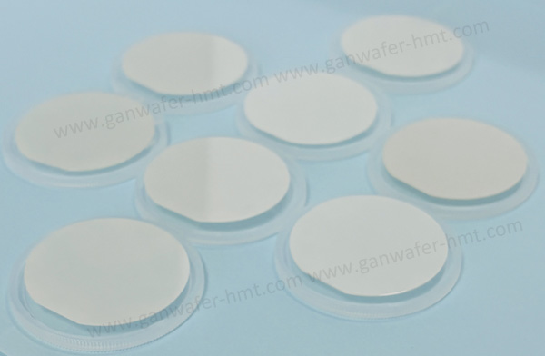
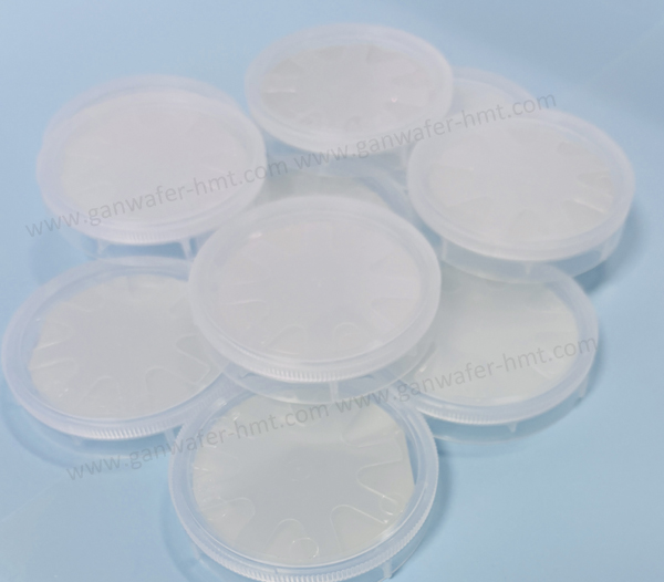
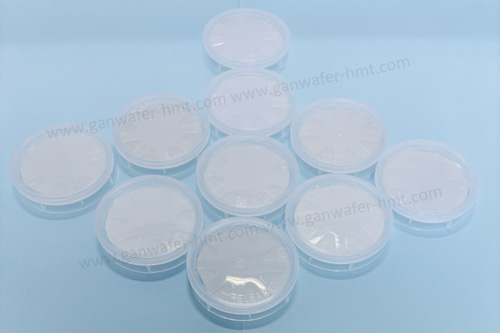
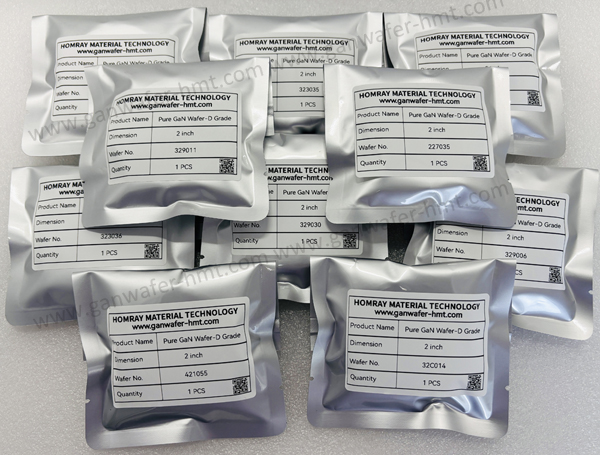
As a leading GaN Substrate Manufacturer, we specialize in the production of high-purity, free-standing GaN wafers(D/R/P Grade), offering exceptional value and the best price on the market. Our standard 2 inch Si-doped N-type thicknesses is 400μm to meet research and production needs.
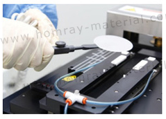
To support the industry's move towards larger formats, we now also provide advanced 6 inch and 8 inch GaN substrates. This expansion in our capabilities ensures we can serve the most demanding applications. If you are looking for a reliable partner for high-quality GaN substrates, please do not hesitate to contact us for more information and pricing.
 Homray Material Technology. All rights Reserved.
![]() E-mail:kim@homray-material.com;tina@homray-material.com
E-mail:kim@homray-material.com;tina@homray-material.com
![]() M.P: +86-15366208370 ; +86-15366203573
M.P: +86-15366208370 ; +86-15366203573