
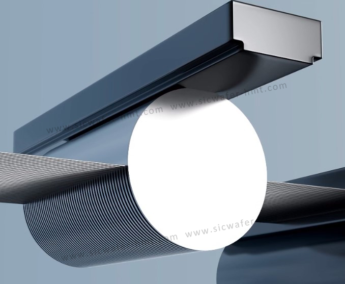
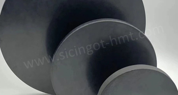
HMT as the professional SiC Wafer Supplier, we offer 2inch to 8inch SiC Boule/Ingot for Slicing testing. Silicon Carbide (SiC), as the core substrate material of third-generation semiconductors, is extremely hard – with a Mohs hardness of 9.2. The mainstream slicing methods in the industry currently include fixed abrasive diamond wire sawing, laser thermal cleavage, and stealth laser dicing, alongside gradually phased-out methods like diamond blade dicing and wire electrical discharge machining (W-EDM). So, which method is truly the best?
The Mainstream Choice
The most commonly used method in the industry today is fixed abrasive
diamond wire sawing, particularly reciprocating and loop-type systems, which are considered the "workhorse" for SiC dicing. Its principle is straightforward: diamond abrasive grains are "bonded" to the cutting wire via methods like electroplating or brazing, and the SiC crystal is "sawn" open by the high-speed motion of the diamond wire. Its core advantages are as follows:
-
High Efficiency: It belongs to "two-body abrasion," making it several times more efficient than traditional free abrasive wire saws. Dicing time for 8-inch SiC wafers can be controlled within one hour.
-
Low Loss: The kerf width is only 50~80μm, much narrower than that of diamond blades, increasing material utilization by over 20%.
-
Environmentally Friendly & Controllable: It doesn't require complex slurry circulation systems, reducing pollution. Cutting parameters are easy to adjust, making it suitable for high-volume mass production.
However, for power device manufacturers prioritizing production efficiency and cost control, fixed abrasive diamond wire sawing remains the current "optimal solution" – mature technology, stable yield, and capable of supporting the mass production of 8-inch SiC wafers. This is the core reason it holds over 80% of the market share.
The Emerging Contenders
Laser dicing is divided into laser thermal cleavage and stealth laser dicing. Both are non-contact processes, perfectly avoiding the "physical damage" issues associated with wire sawing, making them particularly suitable for high-end applications.
1. Laser Thermal Cleavage
The principle is quite ingenious: A laser rapidly irradiates the SiC surface, causing localized instantaneous heating and generating compressive stress. After the laser moves away, the temperature plummets, creating significant tensile stress. When this tensile stress exceeds the material's strength, the material fractures neatly along the laser path.
-
Advantages: The cut surface is smooth with almost no chipping. Furthermore, there is no material loss and no pollution, making it suitable for scenarios requiring high surface quality.
-
Disadvantages: The limitations are also prominent: limited cutting depth – efficiency for thick 8-inch wafers is not as good as wire saws. Additionally, it requires extremely high linearity of the laser path, making curved cuts difficult.
2. Stealth Laser Dicing
This is the most promising emerging technology, and its principle can be called "cutting-edge": Pulsed laser is focused inside the SiC substrate without damaging the surface, forming a "modified layer" internally. Afterward, slight pressure is applied, and the wafer cleaves precisely along this modified layer. Its core advantages directly address key pain points:
-
Extremely Low Material Loss: The kerf width is nearly zero, increasing material utilization by over 30% compared to wire saw dicing.
-
Ideal for Ultra-thinning: It can easily dice wafers as thin as 0.1~0.3mm with no edge chipping or thermal damage.
-
Clean and Pollution-Free: The entire process is free of debris and cutting fluid, significantly reducing subsequent processing costs.
 Homray Material Technology. All rights Reserved.
![]() E-mail:kim@homray-material.com;tina@homray-material.com
E-mail:kim@homray-material.com;tina@homray-material.com
![]() M.P: +86-15366208370 ; +86-15366203573
M.P: +86-15366208370 ; +86-15366203573