
Silicon Carbide (SiC) is a binary compound formed from silicon (Si) and carbon (C) atoms in a 1:1 ratio. It is the foundational material for advanced semiconductors, with leading SiC Wafer Manufacturers producing wafers in standard sizes like 4 inch and increasingly larger 8 inch diameters sicc wafer to meet growing demand. Its fundamental building block is the Si-C tetrahedron.
For analogy, Si atoms are larger, akin to apples, while C atoms are smaller, akin to oranges. Piling an equal number of oranges and apples together forms the SiC crystal.
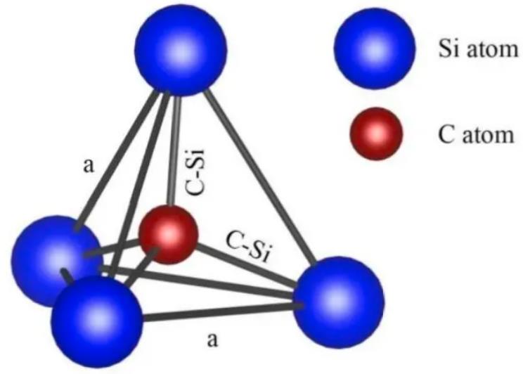
SiC is a binary compound. The atomic spacing of the Si-Si bond is 3.89 Å. How to understand this distance? The current most advanced lithography machines have a resolution of 3nm, which is 30 Å – meaning the lithographic precision is about 8 times this atomic distance.
The Si-Si bond energy is 310 kJ/mol. Bond energy can be understood as the force required to separate the two atoms; a higher bond energy means a greater force is needed to break them apart.
The Si-C bond has an atomic spacing of 1.89 Å and a bond energy of 447 kJ/mol.
The bond energy values indicate that compared to traditional silicon-based semiconductor materials, silicon carbide-based semiconductor materials are chemically more stable.
From the diagram, it can be seen that any C atom is bonded to four nearest neighboring Si atoms, and conversely, any Si atom is bonded to four nearest neighboring C atoms.
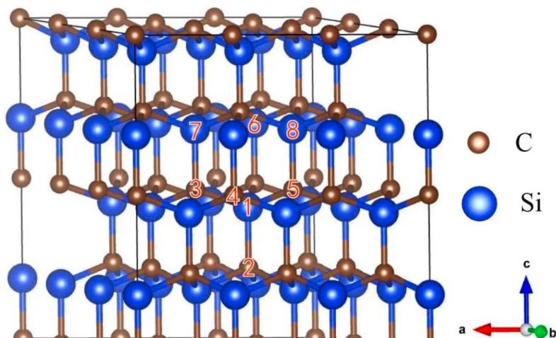
The crystal structure of SiC can also be described using a layered structure approach. As shown in the figure, several C atoms in the crystal occupy the hexagonal lattice sites within the same plane, forming a close-packed C atomic layer. Similarly, Si atoms occupy the hexagonal lattice sites within the same plane, forming a close-packed Si atomic layer.
Every C in the close-packed C atomic layer is bonded to the nearest neighboring Si, and vice versa for the Si atomic layer. Every two adjacent C and Si close-packed atomic layers constitute a carbon-silicon diatomic layer.
The arrangement and combination forms in SiC crystals are highly diverse. Over 200 different SiC polytypes have been discovered so far.
This is somewhat similar to Tetris blocks: although the minimal unit blocks are identical, different shapes are formed when these blocks are combined.
The spatial structure of SiC is slightly more complex than Tetris. Its minimal unit changes from small squares to small tetrahedra, composed of C and Si atoms.
To distinguish between different SiC polytypes, the Ramsdell notation is currently the primary method used. This method uses a combination of numbers and letters to represent different SiC polytypes.
The letter, placed after the number, indicates the crystal system type of the unit cell: C represents the Cubic crystal system, H represents the Hexagonal crystal system, and R represents the Rhombohedral crystal system. The number, placed before the letter, indicates the number of Si-C diatomic layers in the basic repeating unit.
Except for 2H-SiC and 3C-SiC, other polytypes can be regarded as mixtures of the zincblende and wurtzite structures, i.e., a close-packed hexagonal structure.
The C-face refers to the (000-1) crystal plane of the silicon carbide wafer. This is the surface obtained by cutting the crystal along the negative direction of the c-axis, and the terminating atoms on this surface are carbon atoms.
The Si-face refers to the (0001) crystal plane of the silicon carbide wafer. This is the surface obtained by cutting the crystal along the positive direction of the c-axis, and the terminating atoms on this surface are silicon atoms.
The difference between the C-face and Si-face affects the physical and electrical properties of silicon carbide wafers, such as thermal conductivity, electrical conductivity, carrier mobility, and interface state density.
The choice between C-face and Si-face also impacts the manufacturing process and performance of SiC devices, such as epitaxial growth, ion implantation, oxidation, metal deposition, and contact resistance.
 Homray Material Technology. All rights Reserved.
![]() E-mail:kim@homray-material.com;tina@homray-material.com
E-mail:kim@homray-material.com;tina@homray-material.com
![]() M.P: +86-15366208370 ; +86-15366203573
M.P: +86-15366208370 ; +86-15366203573