
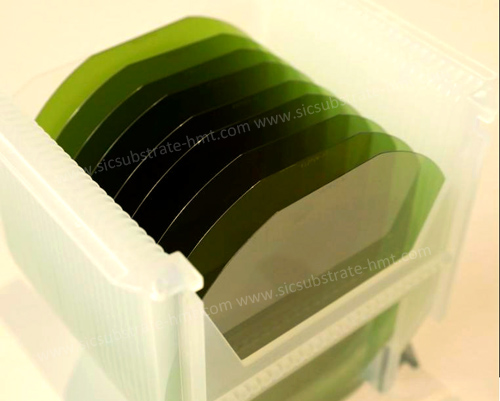
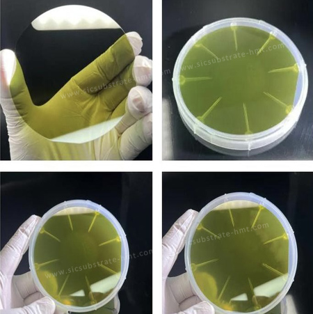
6''8'' P Type SiC Epi Wafer Manufacturer
Size: 6'' 8''
Type: P-Type
Dopant: Aluminum
Thickness:0.2~50μm
Product Description
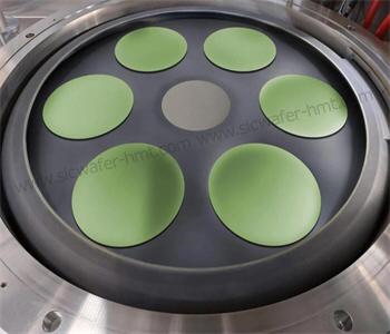
What is SiC Epi Wafer? Let professional SiC Wafer Manufacturer HMT tell you. A silicon carbide(SiC) epitaxial(Epi) wafer refers to the epitaxial growth of a single-crystal SiC thin film on the substrate surface, forming the active layer of the device. We can grow 6''8'' Aluminum P Type SiC Epi Layer and 4inch 6inch 8inch Nitrogen N Type Epi Layer.
The growth of a SiC Epi layer on a conductive N Type SiC substrate (thickness 350um) produces a SiC homoepitaxial wafer, which can be further processed into power devices such as Schottky barrier diodes, MOSFETs, and IGBTs. Among these, 4H-SiC is the most widely used. The thickness of the epi layer ranges from a few micrometers to over a hundred micrometers, and its doping concentration and crystal quality directly impact the final chip performance.
SiC Epi Wafer Basic Spec
- Dimension: 6inch,8inch
- Substrate: Production Grade SiC Wafer
- Substrate Thickness: 350±25um/ 500±25um
- Epi Layer Dopant: Aluminum
- Epi Layer Thickness:0.2~100um
- Bufffer : N type 1μm 1E18cm-3
Related Products

 Homray Material Technology. All rights Reserved.
![]() E-mail:kim@homray-material.com;tina@homray-material.com
E-mail:kim@homray-material.com;tina@homray-material.com