
GaN Epitaxial On SiC For Power HEMT
GaN-On-SiC Epi Wafer For Power HEMT
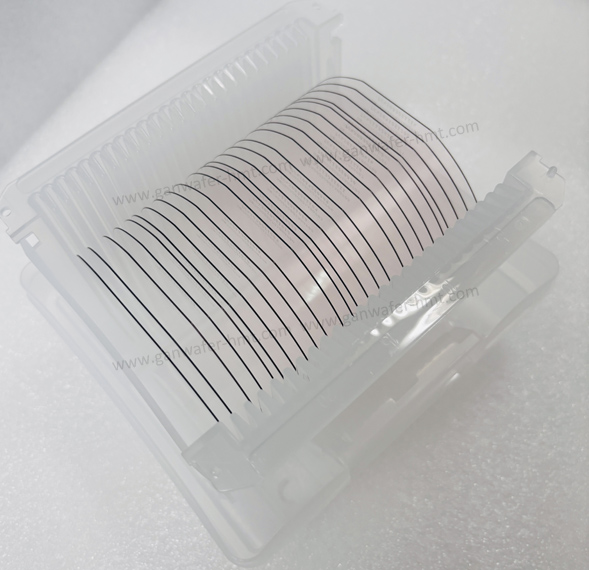
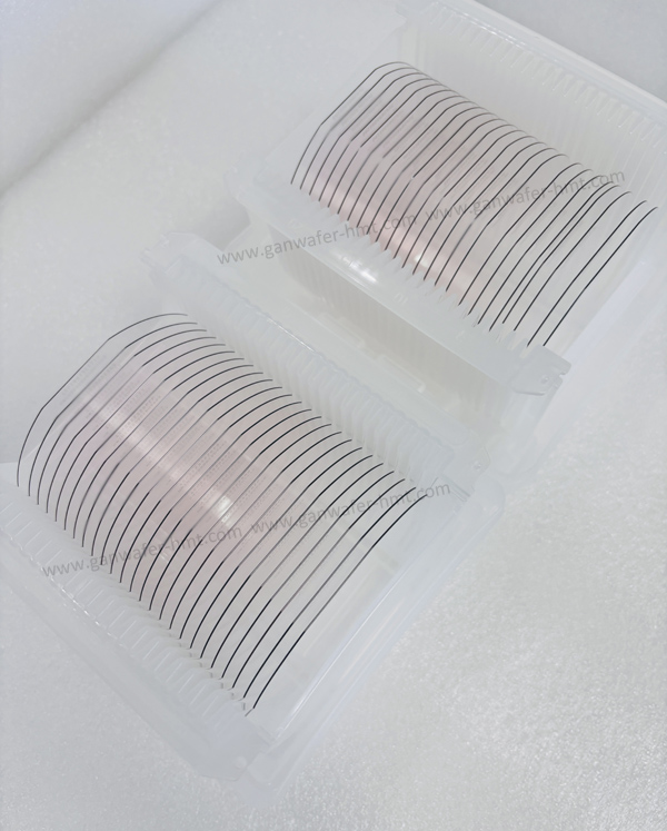
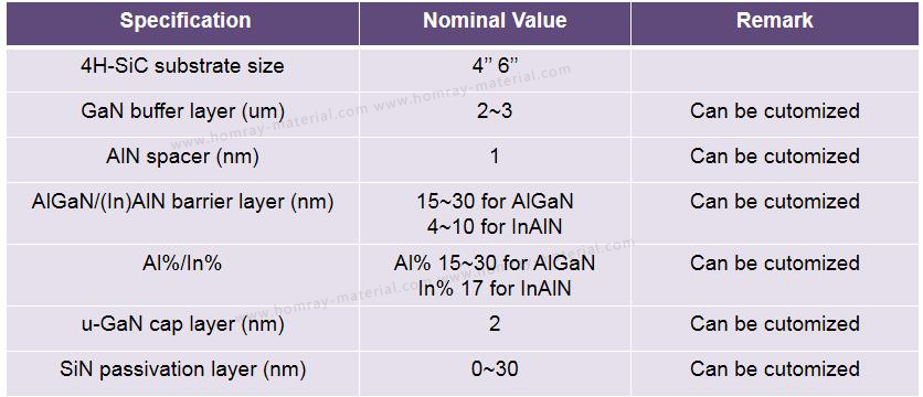
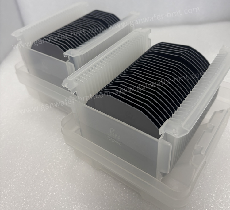
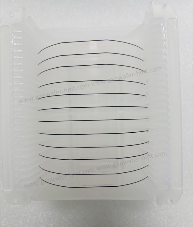
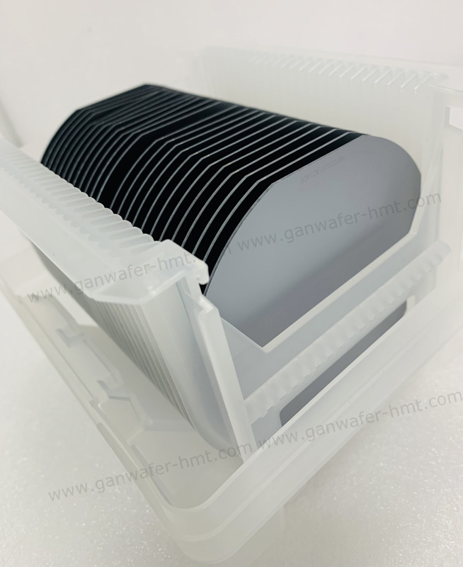
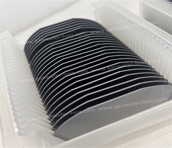
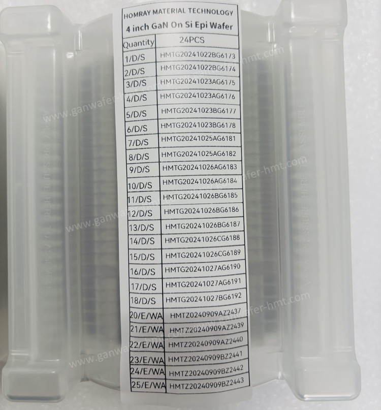
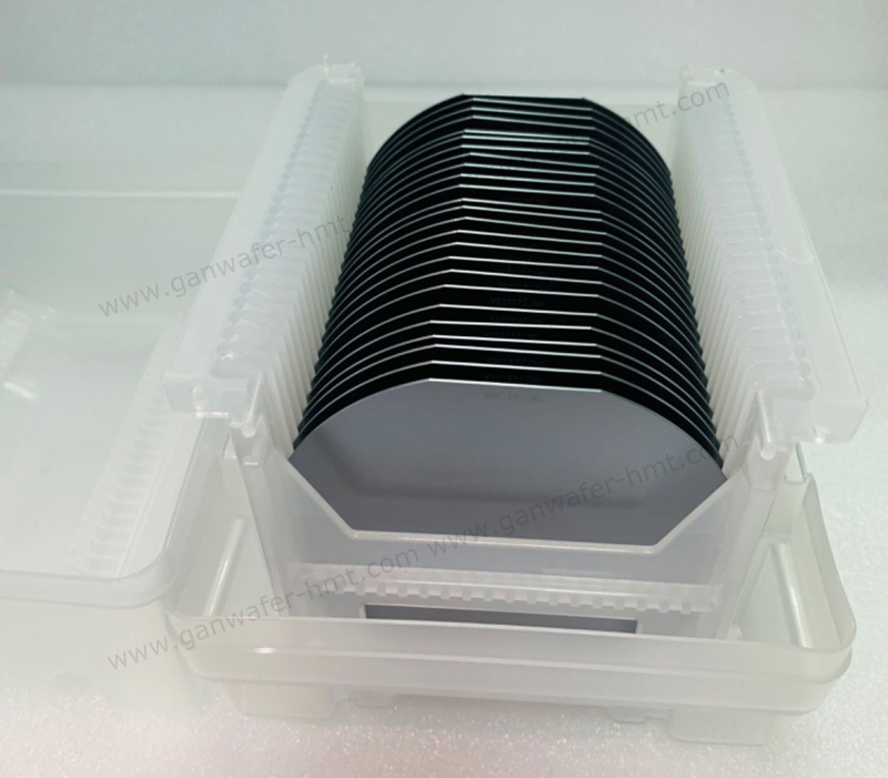
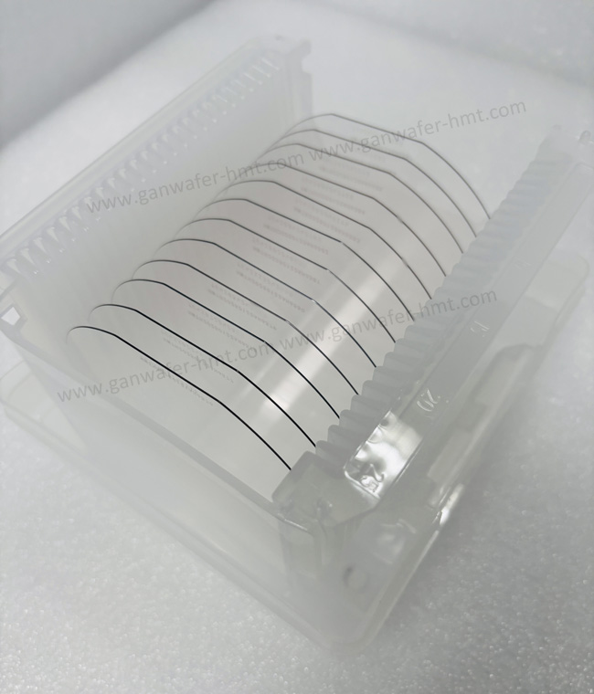
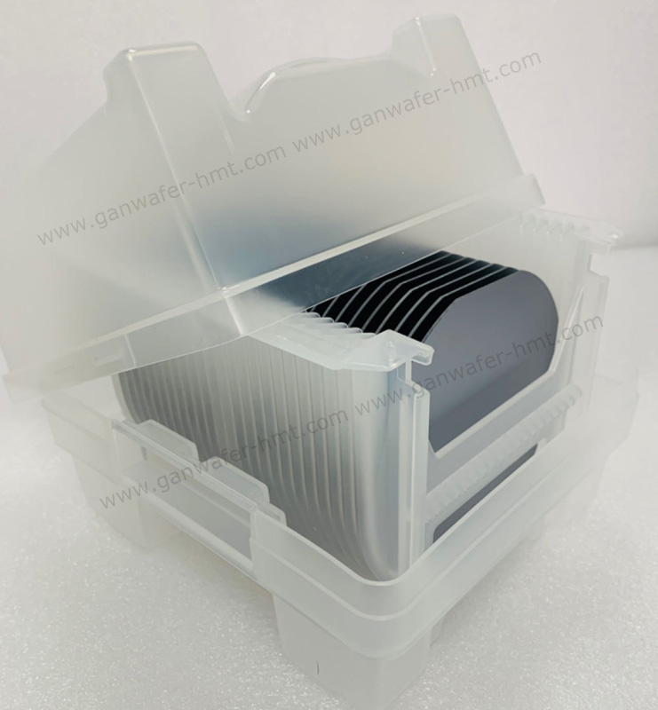
Substrate Size: 4''6''
Substrate Thickness: 500um
GaN Buffer Layer: 2-3um
Product Description
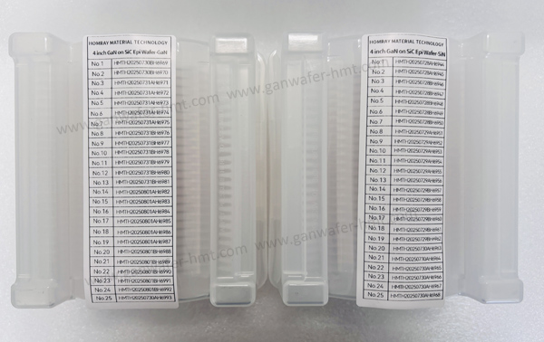
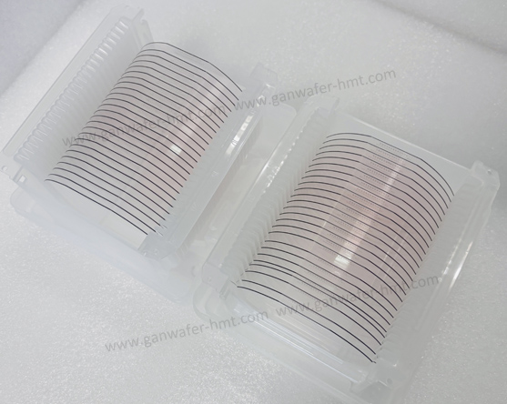
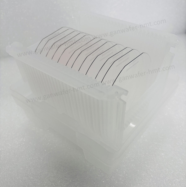
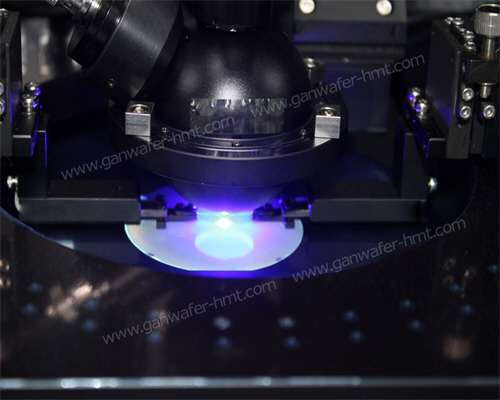
As the industry leading manufacturer of GaN Epi Wafers, 100mm and 150mm GaN Epi wafers on SiC substrates both available in HMT company. Our GaN-on-SiC Epi wafers are grown by the MOCVD process. We have complete and independent supporting system, including epi growth,clean,test and maintain equipments. We also have GaN on SiC For RF structures with best price on the market.
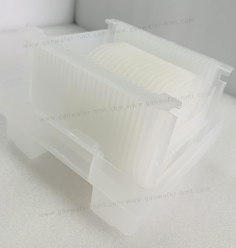
HMT company has highly automated quality control and manufacturing management systems installed and running across the Fab. HMT follow strict manufacturing procedures and production quality control to meet and exceed customer’s expectations and product specifications.
Standard Layer Structure For Power HEMT
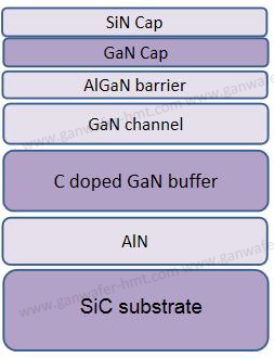
Standard Layer Specification
Related Products
 Homray Material Technology. All rights Reserved.
![]() E-mail:kim@homray-material.com;tina@homray-material.com
E-mail:kim@homray-material.com;tina@homray-material.com
![]() M.P: +86-15366208370 ; +86-15366203573
M.P: +86-15366208370 ; +86-15366203573