
HEMT GaN On SiC For Power Wafer Manufacturers
Type:For Power HEMT
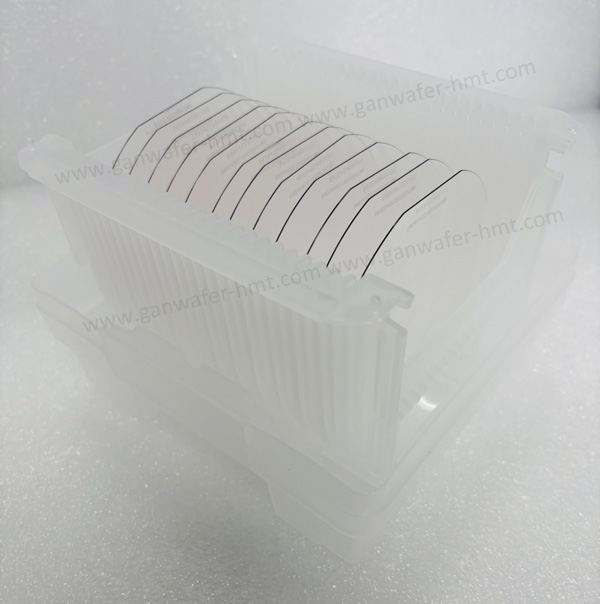
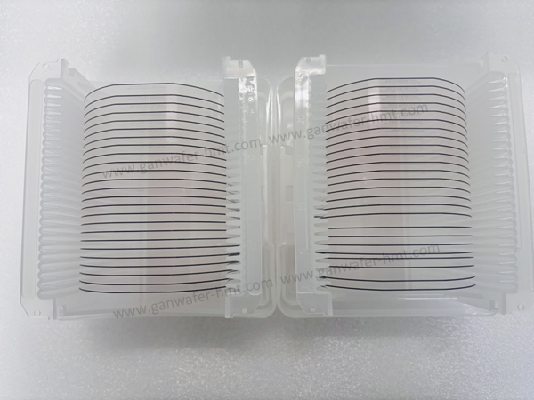
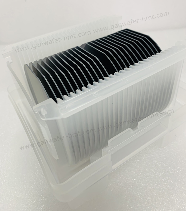
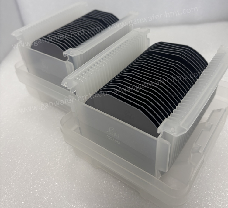
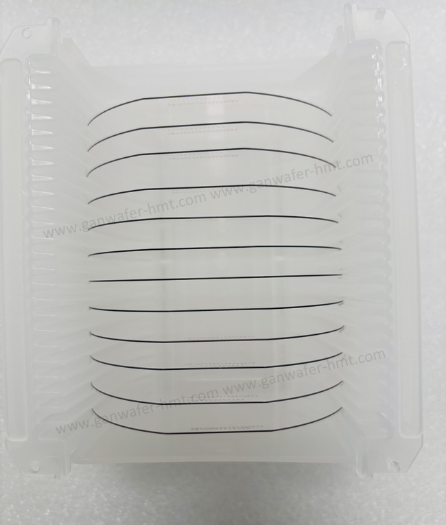
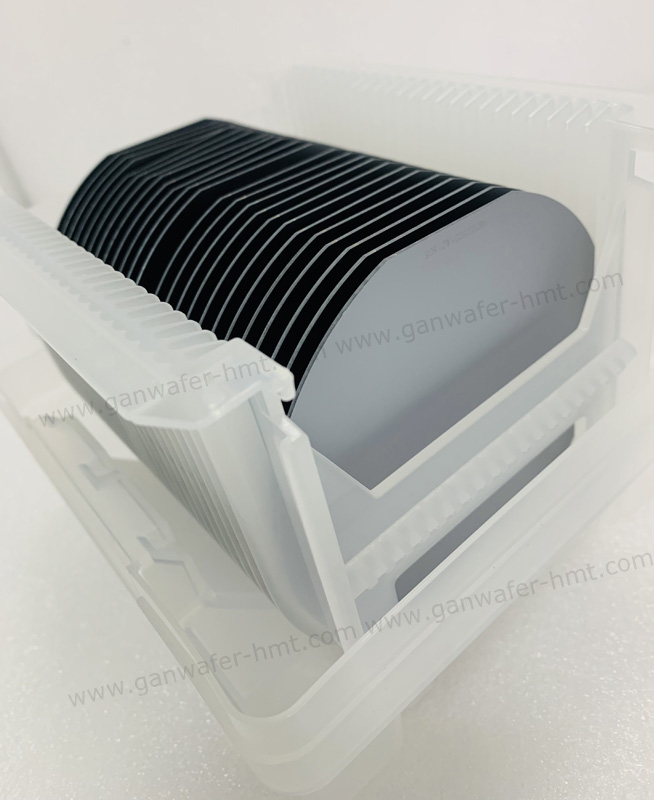
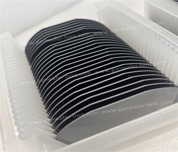
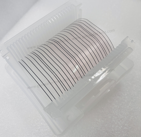
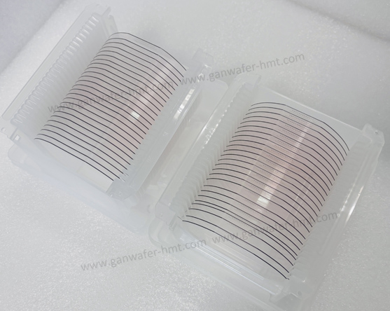
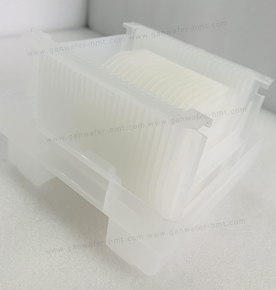
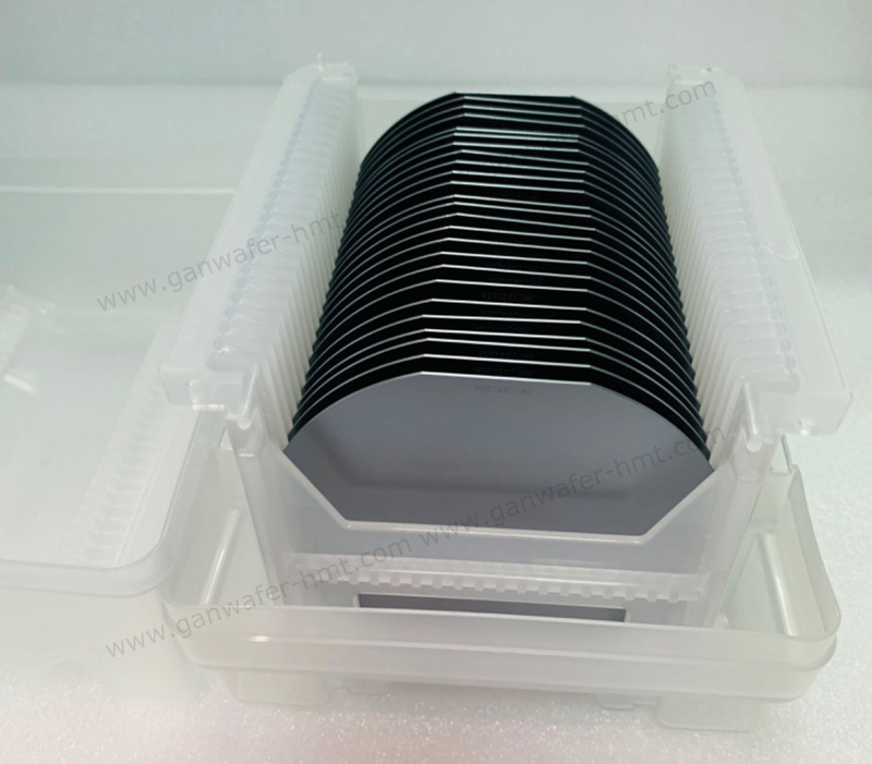
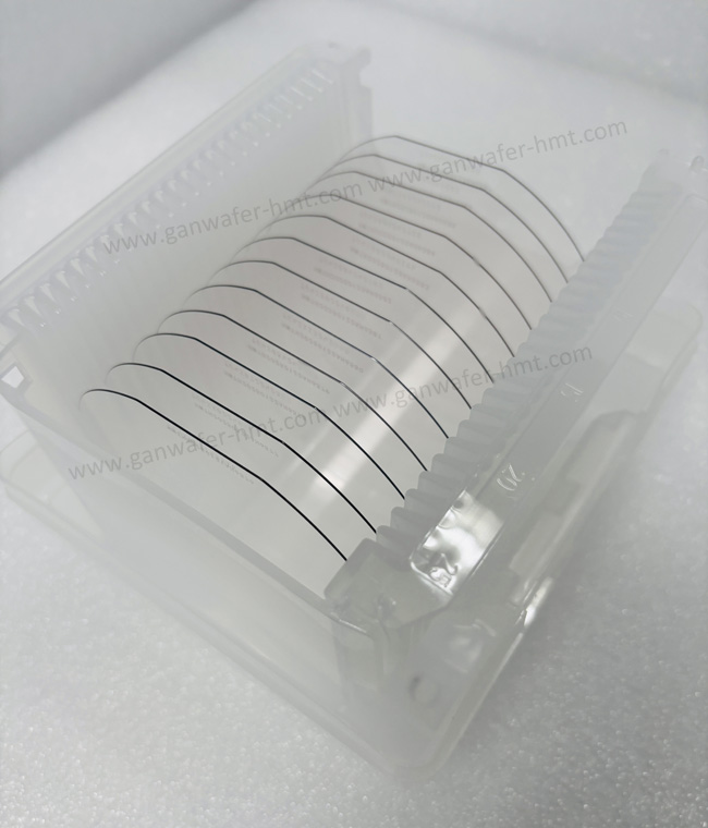
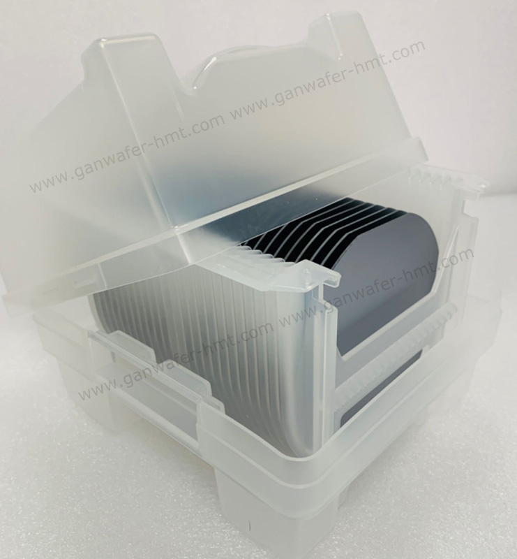
Substrate Diameter: 4 inch, 6 inch
Substrate Thickness: 500um
Substrate Type: Semi-insulating
Product Description
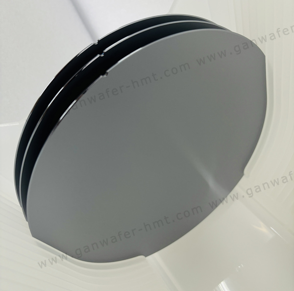
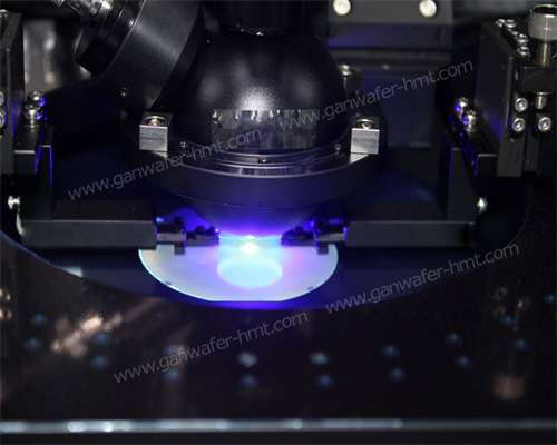
Optimized for high-voltage and high-efficiency power electronics, GaN Epitaxy Wafers Manufacturer--HMT's HEMT GaN-on-SiC Epi Wafers with 4inch and 6inch are engineered to meet the demands of next-generation energy systems, electric vehicles (EVs), and industrial power converters. These wafers combine the superior electrical properties of gallium nitride (GaN) with the unmatched thermal performance of silicon carbide (SiC), enabling devices to operate at higher frequencies, voltages, and temperatures than traditional silicon-based solutions.
Technical Specifications
Diameter: 4-inch (100 mm) / 6-inch (150 mm).
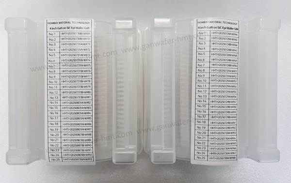
Substrate: High Quality 4H Semi-insulating SiC
SiC Substrate Thickness: 500 µm ±25 µm.
Cap Layer: GaN Cap/SiN Cap/p-GaN Cap
Customize GaN on SiC Epitaxy Wafer GaN Cap and SiN Cap
-
-
Applications
-
Electric Vehicles: Traction inverters, on-board chargers, and DC-DC converters.
-
Renewable Energy: Solar inverters, wind turbine converters.
-
Industrial Systems: Uninterruptible power supplies (UPS), motor drives.
-
-
Related Products
 Homray Material Technology. All rights Reserved.
![]() E-mail:kim@homray-material.com;tina@homray-material.com
E-mail:kim@homray-material.com;tina@homray-material.com
![]() M.P: +86-15366208370 ; +86-15366203573
M.P: +86-15366208370 ; +86-15366203573