
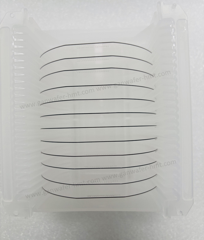
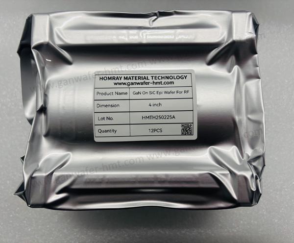
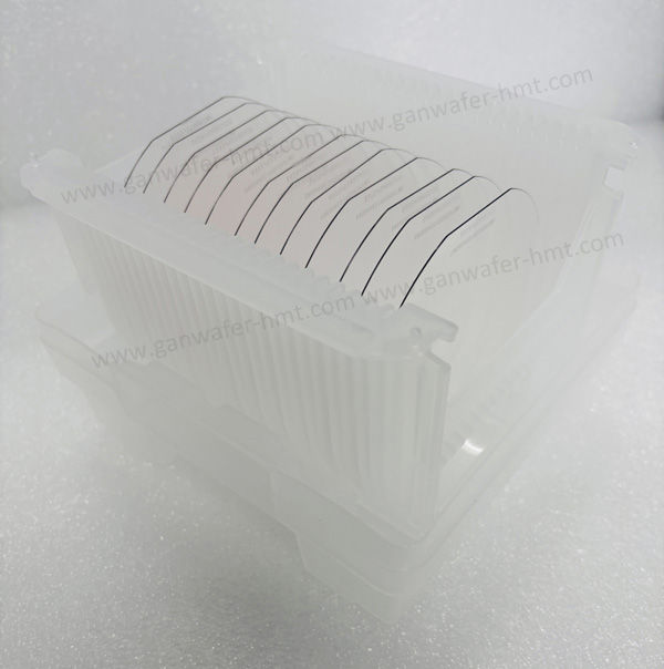
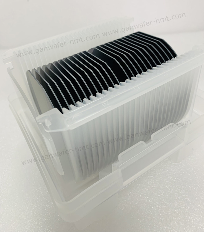
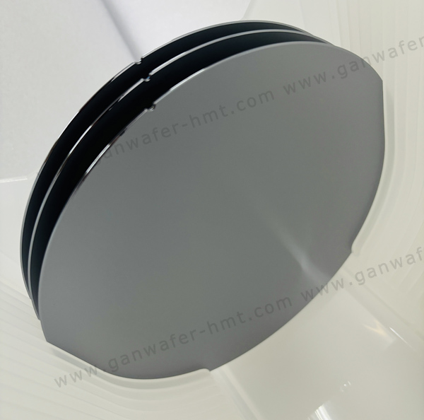
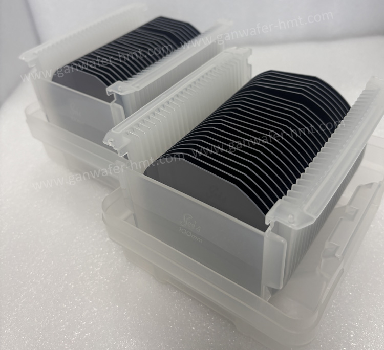
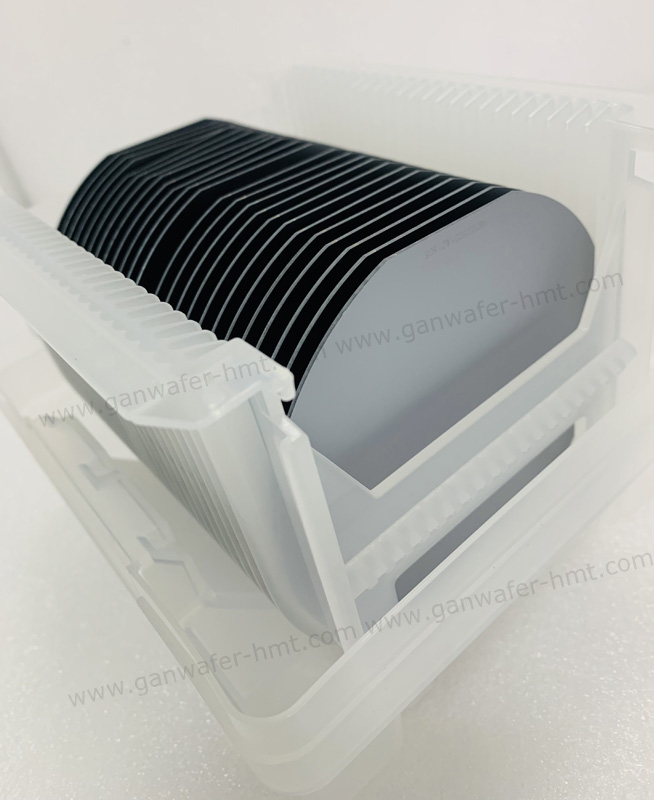
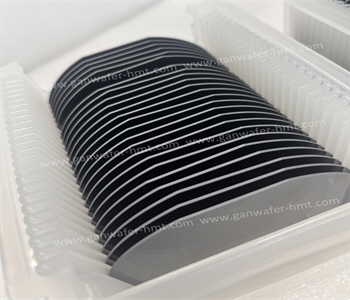
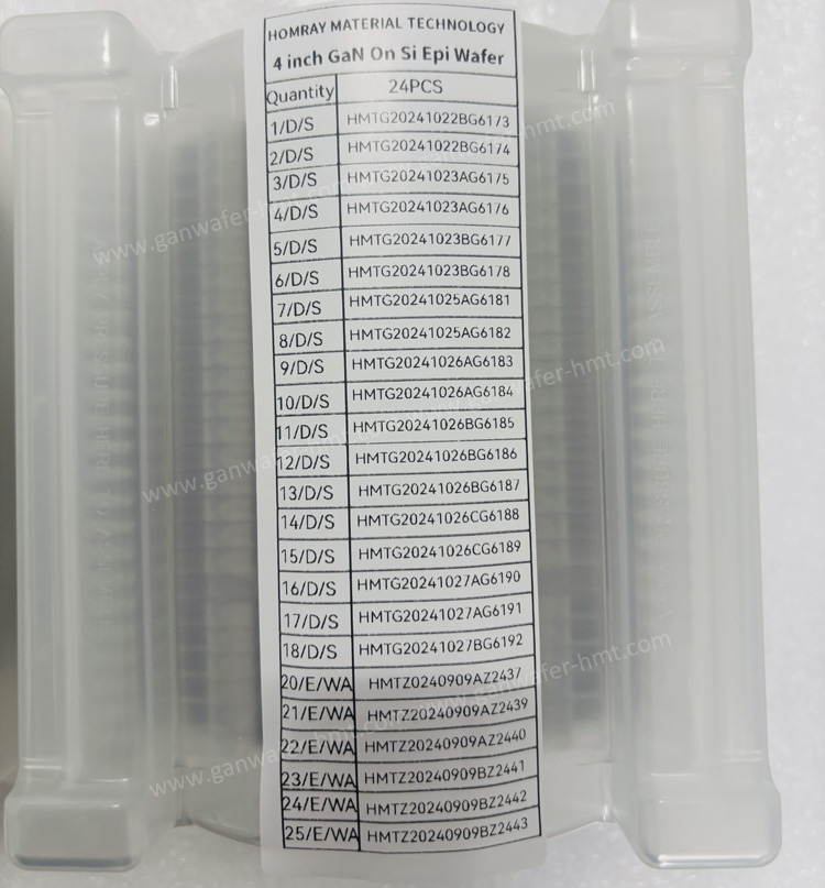
4 inch 4” GaN On SiC Epi Wafer Producers
Type:For Power HEMT or RF
Substrate Diameter: 4 inch, 6 inch
Substrate Thickness: 500um
Substrate Type: Semi-insulating
Product Description
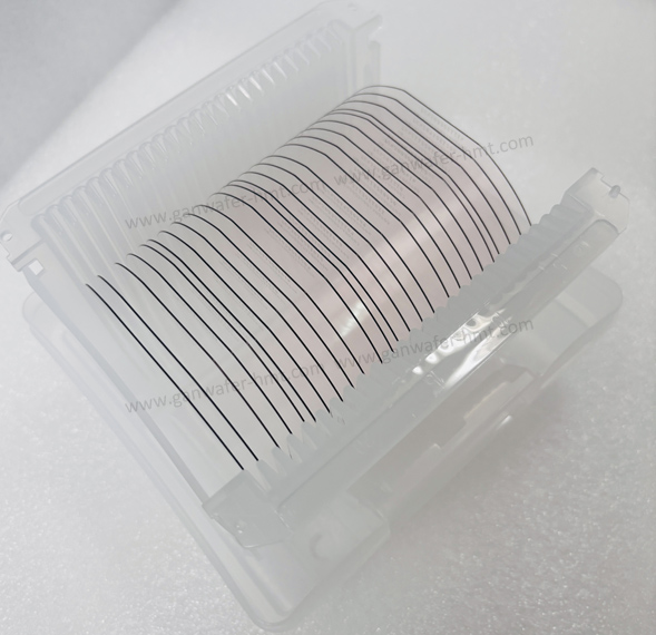
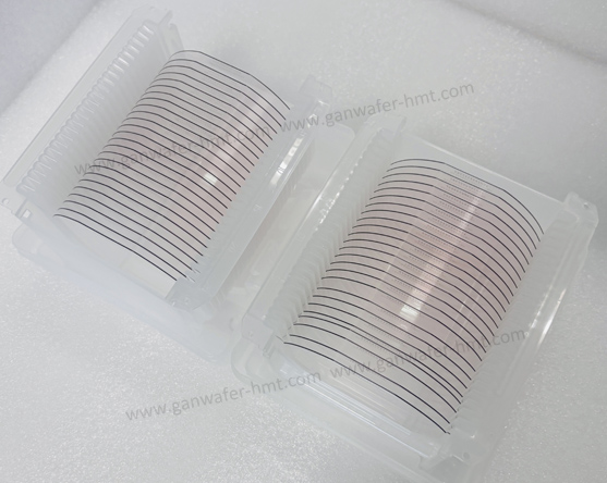
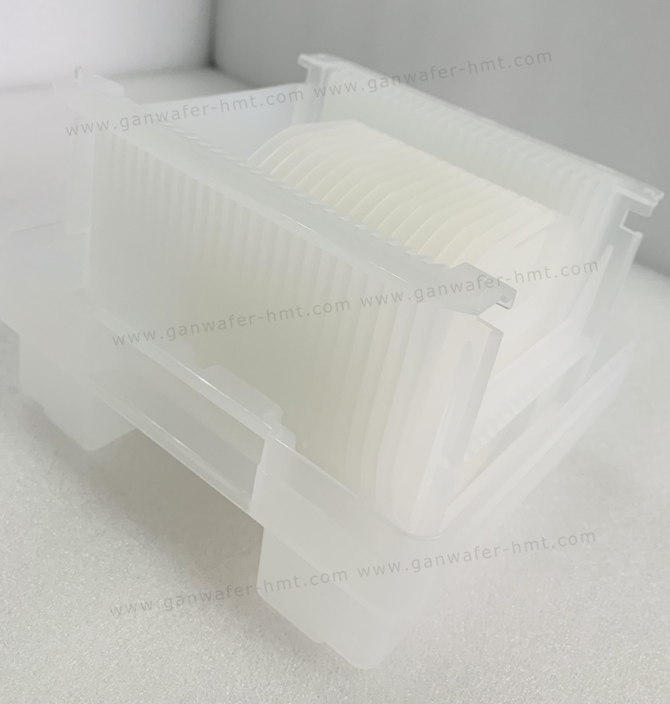
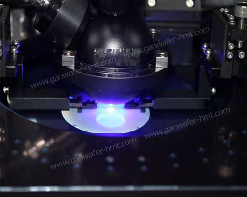
Homray Material specializes in producing high-quality 4-inch GaN-on-SiC epitaxial wafers, designed for advanced RF and power electronics applications. We have both Power HEMT and RF AlGaN/GaN on SiC structures. For example, Rs<350Ω/sq, Carrier Density>9E12cm-2 and Carrier moblity>1600cm2/Vs. These wafers leverage the exceptional material properties of silicon carbide (SiC) and gallium nitride (GaN) to deliver superior performance in high-frequency, high-power environments such as 5G base stations, radar systems, and satellite communications
 Key Advantages of GaN-on-SiC
-
Unmatched Thermal Management
-
SiC substrates exhibit 3x higher thermal conductivity (≥370 W/m·K) compared to silicon (Si), enabling efficient heat dissipation and stable operation at high power densities.
-
Reduced thermal stress and improved reliability for high-temperature applications (e.g., aerospace, defense).
-
-
-
Crystal Quality & Scalability
-
Minimal lattice mismatch (~3.5%) between GaN and SiC ensures high-quality epitaxial growth, reducing defects and enhancing device longevity
-
Compatible with 6-inch wafer production lines, offering cost-effective scalability for mass production.
-
-
Applications
-
RF HEMTs: Ideal for 5G PA, radar, and satellite systems due to high power density and linearity.
-
Power Electronics: Supports D-mode/E-mode devices for electric vehicles (EVs) and renewable energy systems
Contact Us
For quotes or technical inquiries
-
Related Products

 Homray Material Technology. All rights Reserved.
![]() E-mail:kim@homray-material.com;tina@homray-material.com
E-mail:kim@homray-material.com;tina@homray-material.com
![]() M.P: +86-15366208370 ; +86-15366203573
M.P: +86-15366208370 ; +86-15366203573