
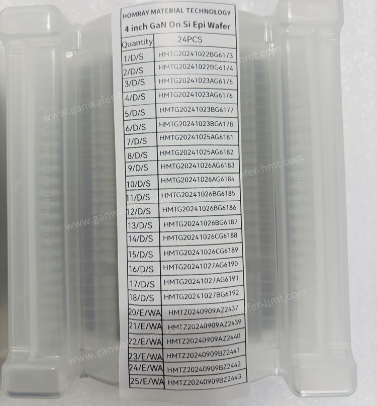
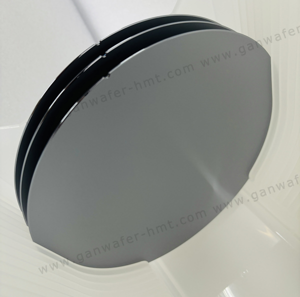
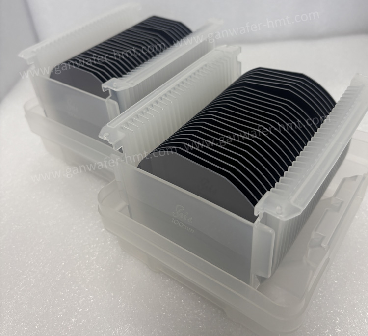
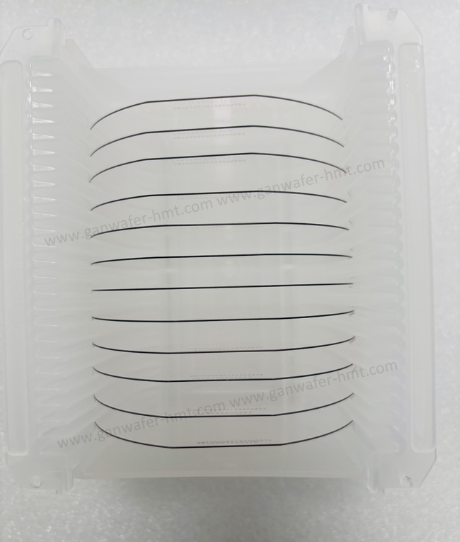
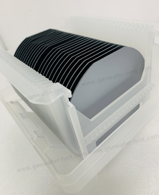
4” GaN On Si (Silicon) HEMT Epi Wafer Producers
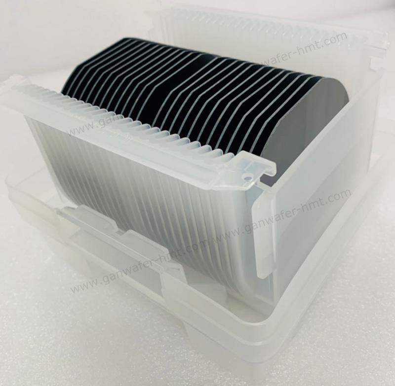
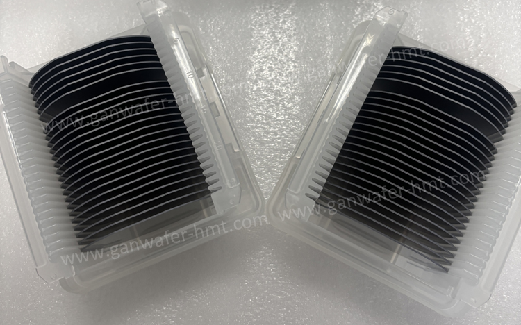
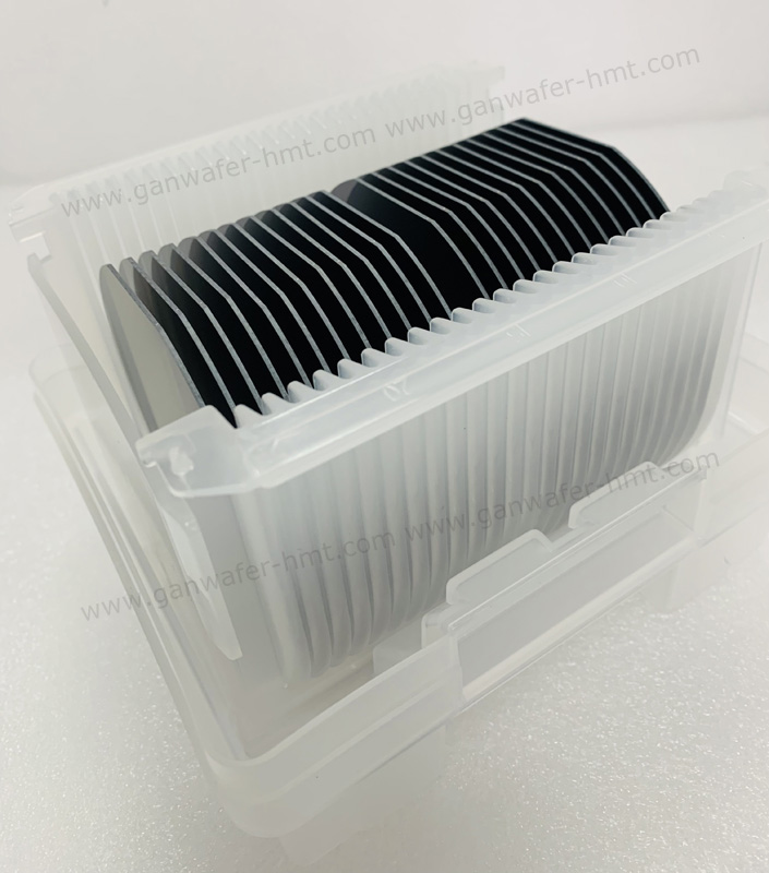
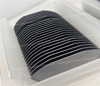
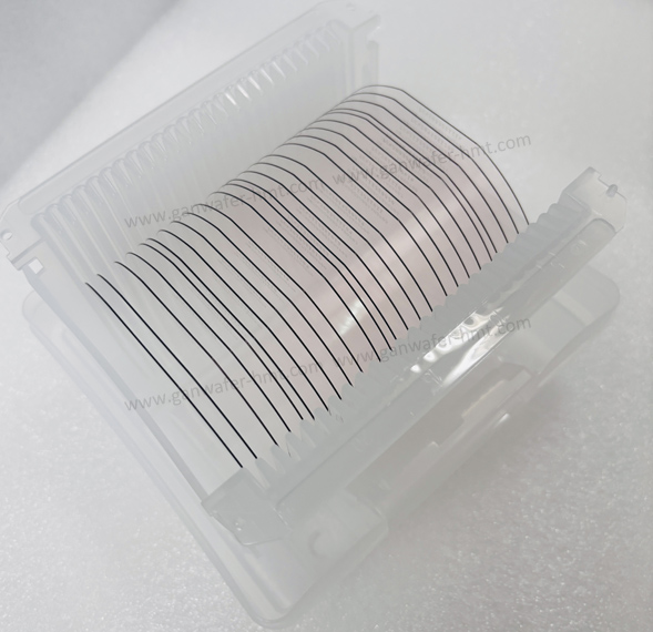
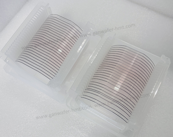
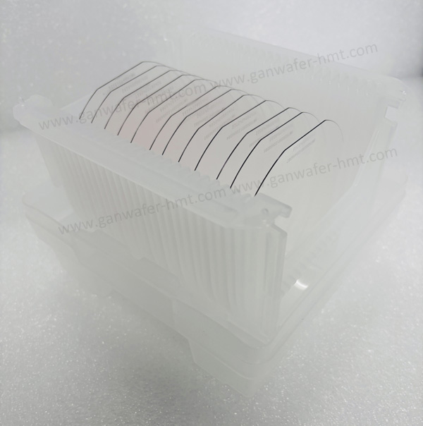
GaN-On-Si Epi Wafer
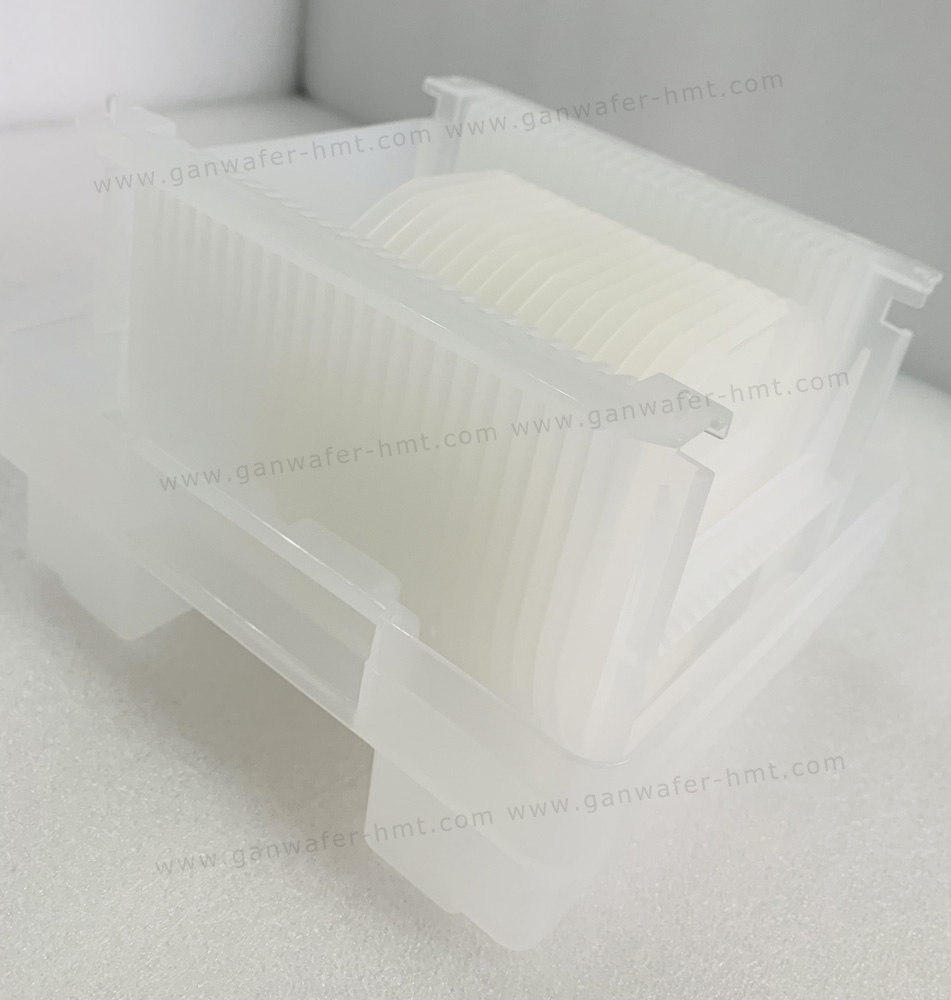
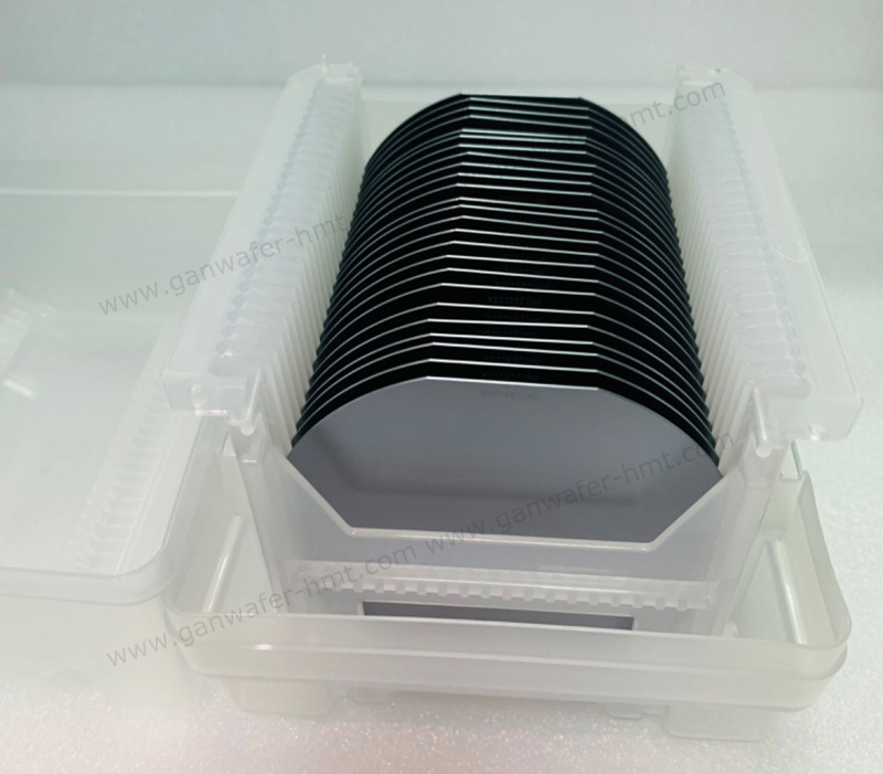
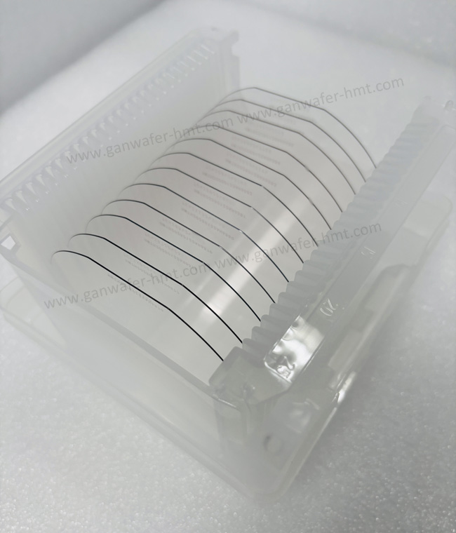
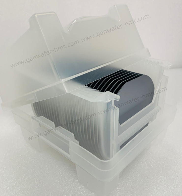
Substrate Diameter: 4inch,6inch,8inch
Substrate Thickness: 675um,1000um
Cap Layer: SiN/GaN/p-GaN
Product Description
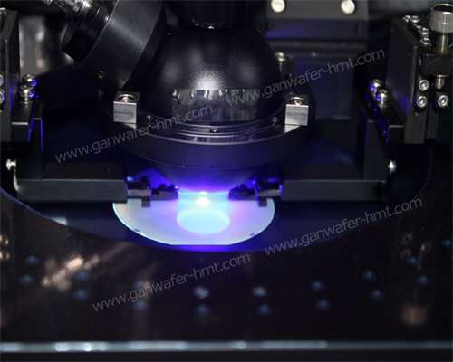
As a trusted producer of GaN-on-Si HEMT (High Electron Mobility Transistor) epiwafers, we deliver all dimensions from 2inch 4inch to 6inch 8inch GaN Epi Wafers to meet the demands of high-frequency, high-power, and high-efficiency applications. Our wafers integrate advanced AlN buffer layers and optimized GaN heterostructures, ensuring superior performance and reliability in even the most challenging environments.
The appropriate substrate material is the guarantee for obtaining epitaxial layer films with high crystallization quality. The selection of substrates usually needs to take into account factors such as the quality of the substrate material itself, the differences in lattice constants and thermal expansion coefficients between the substrate material and the epitaxial material, the size of the substrate material, and the cost.
Generally, the selection of substrate materials is based on the following key conditions:
(1) High Chemical Stability
Epitaxial growth is typically performed at high temperatures. If the substrate lacks sufficient chemical stability—for example, decomposing at elevated temperatures—the released atoms may act as unintended dopants in the epitaxial layer, compromising its properties. Therefore, excellent chemical stability is essential for high-quality epitaxial growth.
(2) Minimal Thermal and Lattice Mismatch
-
Lattice mismatch refers to the difference in lattice constants between the substrate and epitaxial material.
Thermal mismatch refers to the difference in thermal expansion coefficients.
Excessive mismatch can introduce high dislocation densities in the epitaxial film, degrading its quality and potentially rendering it unsuitable for device applications.
(3) Large Size and Low Cost
For large-scale commercial production, cost efficiency is critical. Beyond the substrate’s intrinsic cost, its size determines:
-
The dimensions of the epitaxial film.The number and integration density of devices fabricated on a single wafer.Larger substrates improve material utilization and reduce overall costs.
Related Products
 Homray Material Technology. All rights Reserved.
![]() E-mail:kim@homray-material.com;tina@homray-material.com
E-mail:kim@homray-material.com;tina@homray-material.com
![]() M.P: +86-15366208370 ; +86-15366203573
M.P: +86-15366208370 ; +86-15366203573