
AlGaN/GaN On Si Epi Wafer (AlN Buffer) Manufacturer
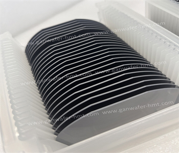
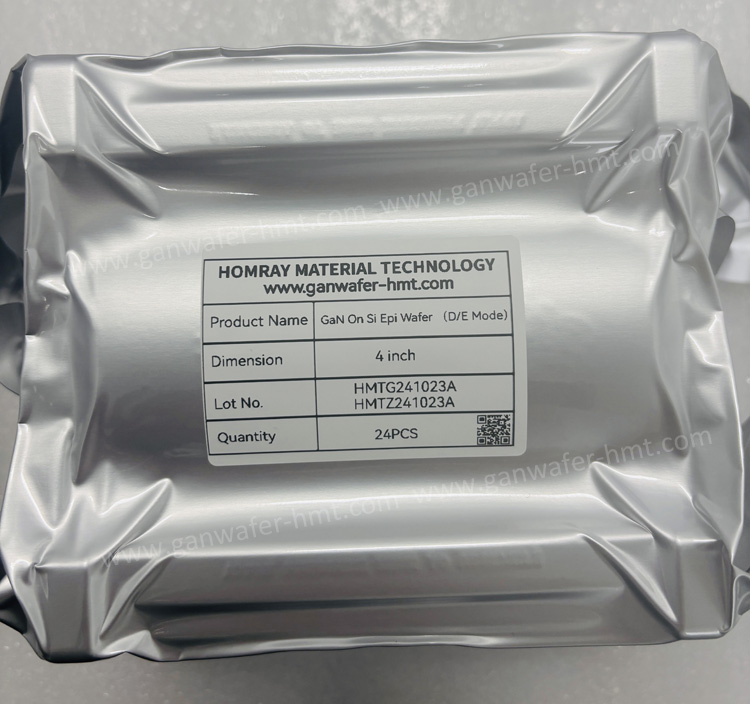
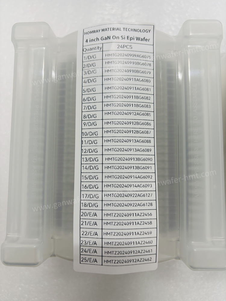
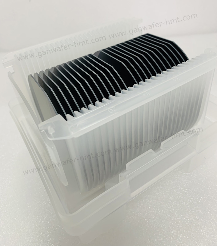
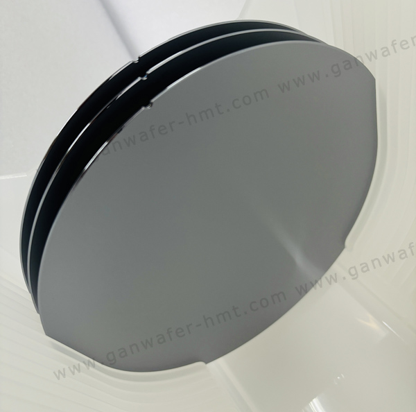
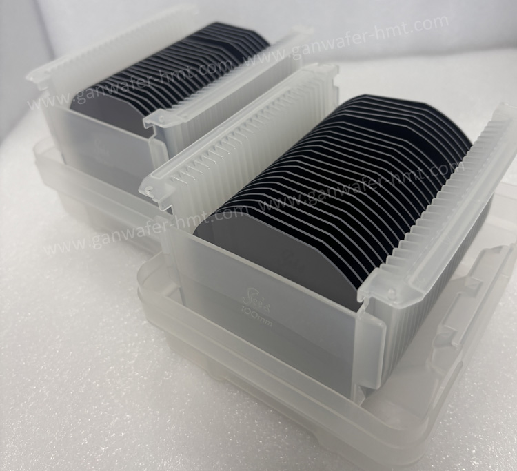
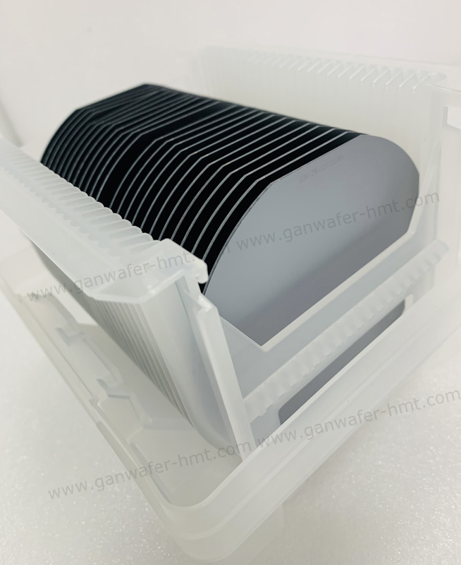
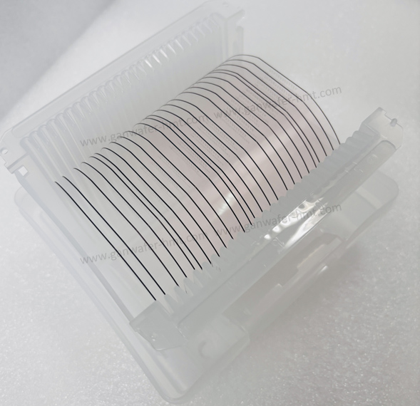
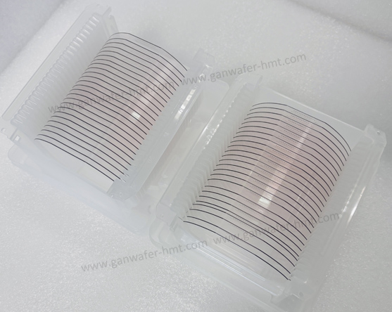
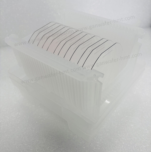
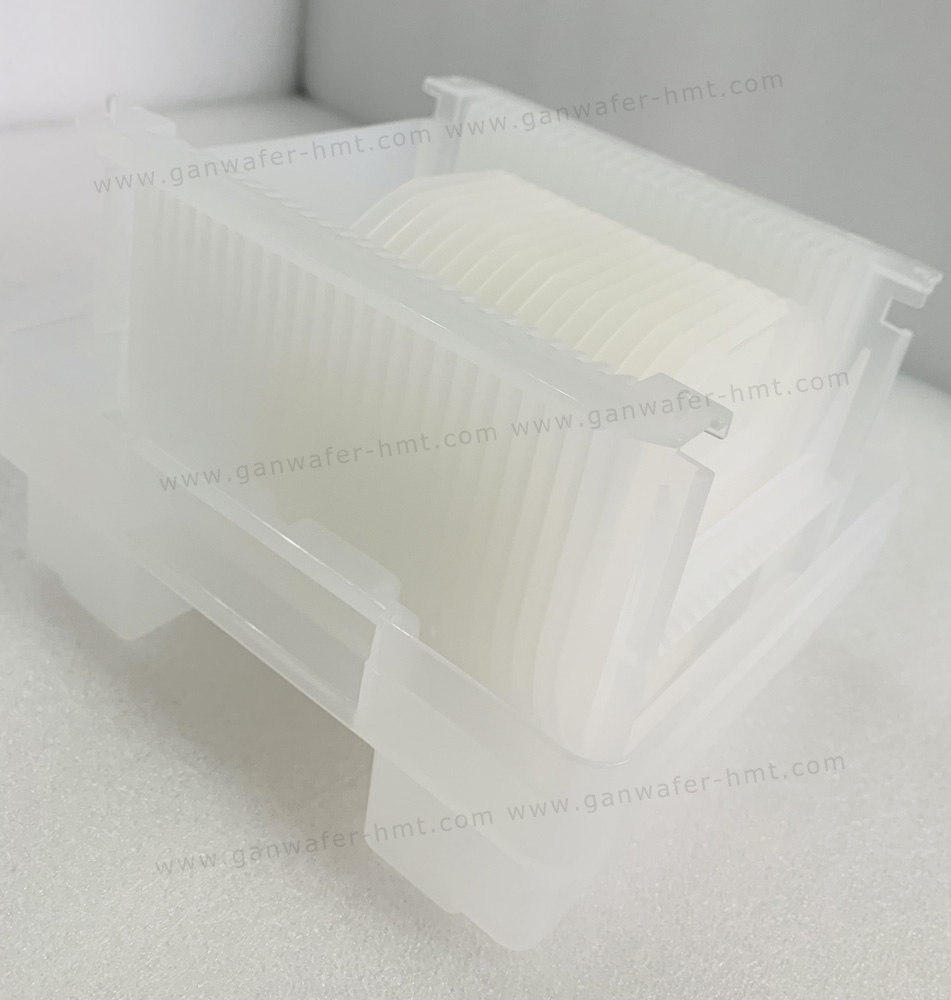
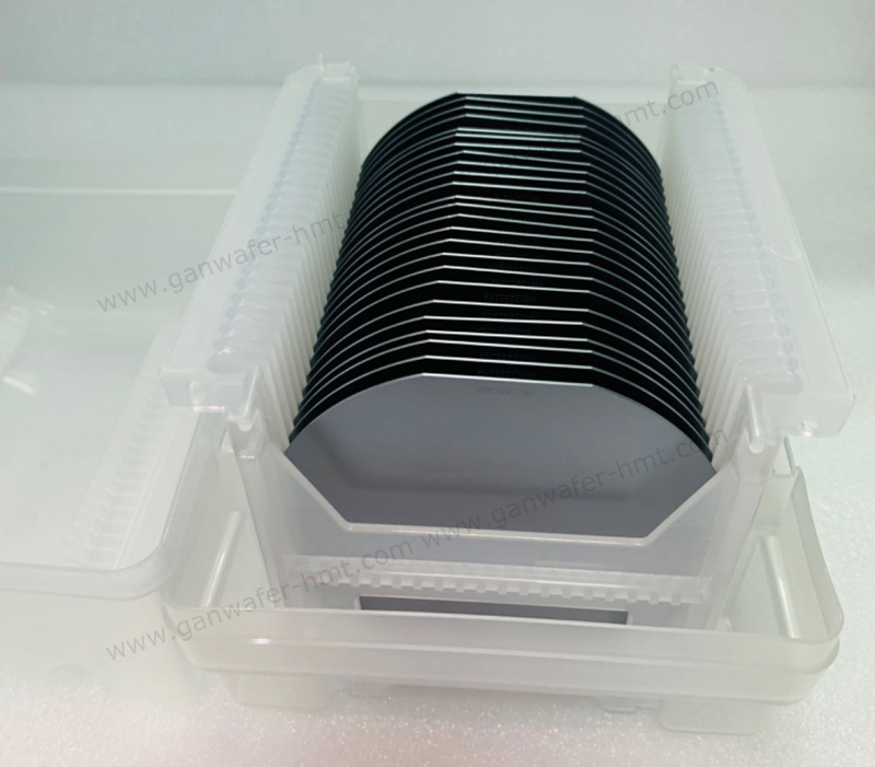
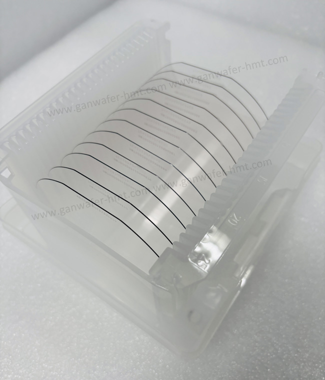
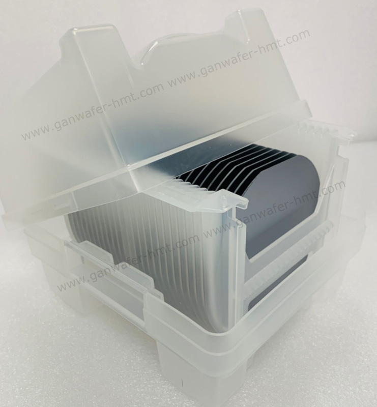
GaN on Si Epi Wafer
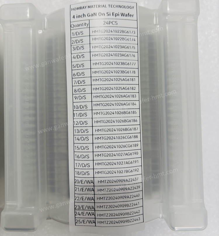
Dimension: 4 inch 6 inch 8 inch
Substrate Thichkness: 675um 1000um
Cap Layer:SiN or GaN cap
Product Description
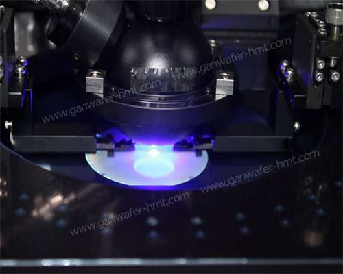
Purchase next-generation semiconductorwith our AlGaN/GaN on Si epitaxial wafers, engineered with a proprietary AlN buffer layer for unmatched reliability and efficiency. We produce 4inch 6inch and 8inch GaN on Si epi wafers for high-frequency, high-power, and high-temperature applications by MOCVD, these wafers combine cutting-edge materials science with precision manufacturing.
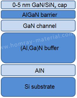
Structure & Design:
-
Substrate: We use p-type <111> orientation Si Substrate.
-
Buffer Layer: Ultra-thin AlN (Aluminum Nitride) to minimize lattice mismatch and thermal stress.
-
Epitaxial Layers: Optimized AlGaN/GaN heterostructure for enhanced 2DEG mobility.
-
Cap Layers: SiN cap layer,GaN cap layer or p-GaN cap layer.
Applications:
-
RF Amplifiers & 5G Base Stations
-
High-Efficiency Power Converters (EVs, Solar Inverters)
-
UV Optoelectronics & Sensors
-
Military & Aerospace Systems
Why Choose Us?
-
MOCVD Expertise: State-of-the-art growth technology for precise layer control.
-
Fast Delivery: Short lead times for R&D and volume orders.
Elevate your semiconductor devices with our industry-leading AlGaN/GaN on Si wafers. Request a datasheet or sample today!
Related Products
 Homray Material Technology. All rights Reserved.
![]() E-mail:kim@homray-material.com;tina@homray-material.com
E-mail:kim@homray-material.com;tina@homray-material.com
![]() M.P: +86-15366208370 ; +86-15366203573
M.P: +86-15366208370 ; +86-15366203573