
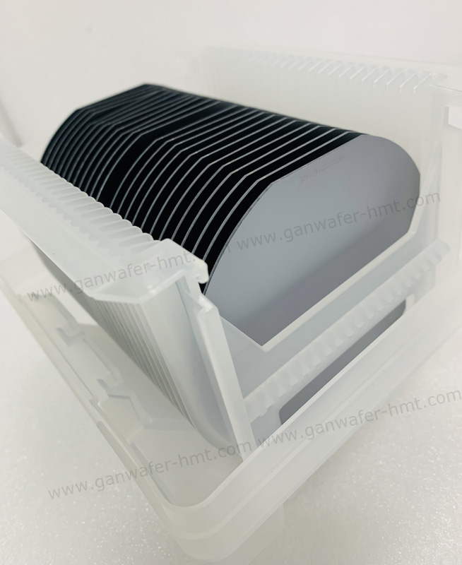
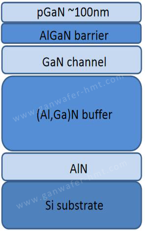
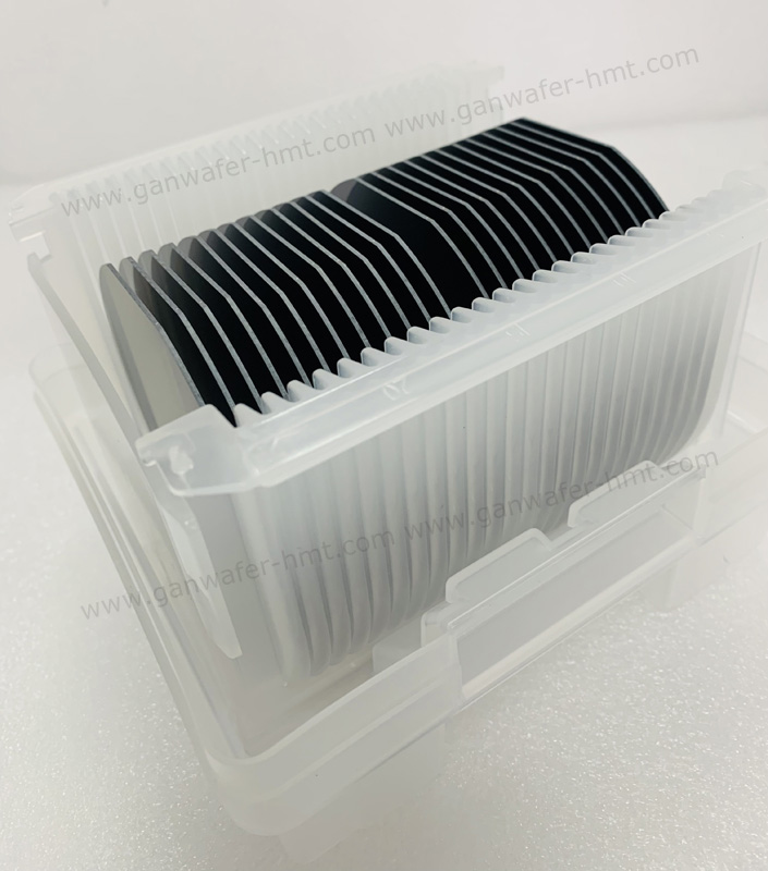
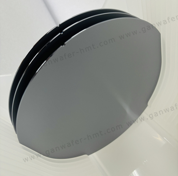
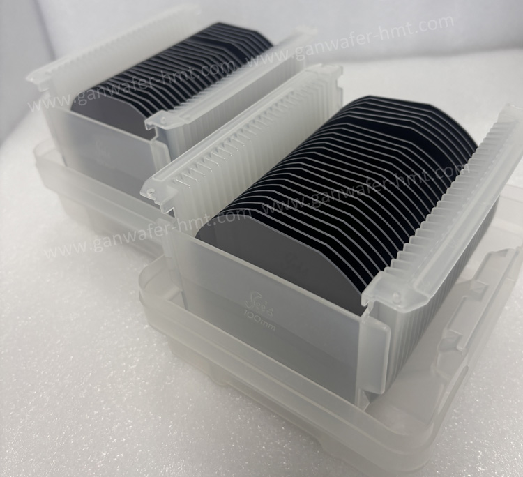
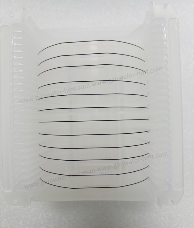
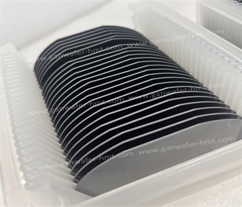
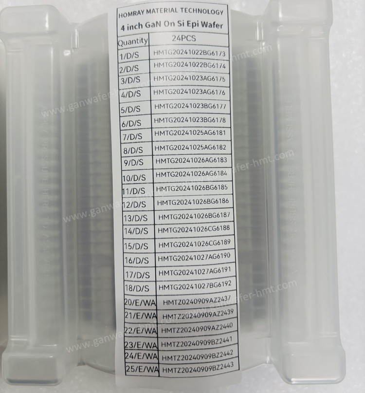
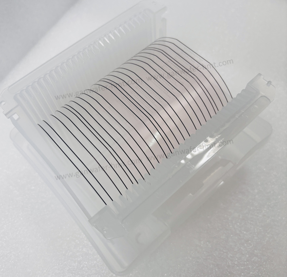
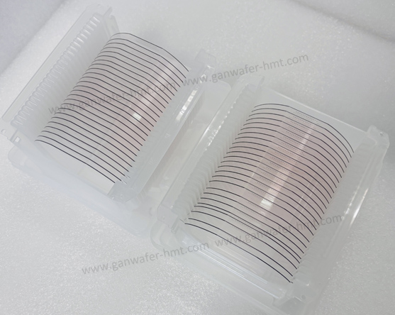
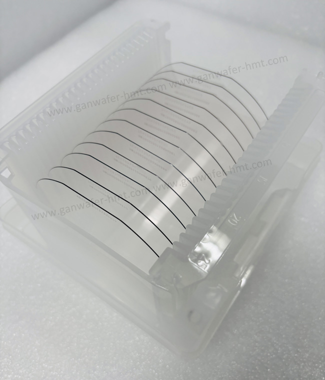
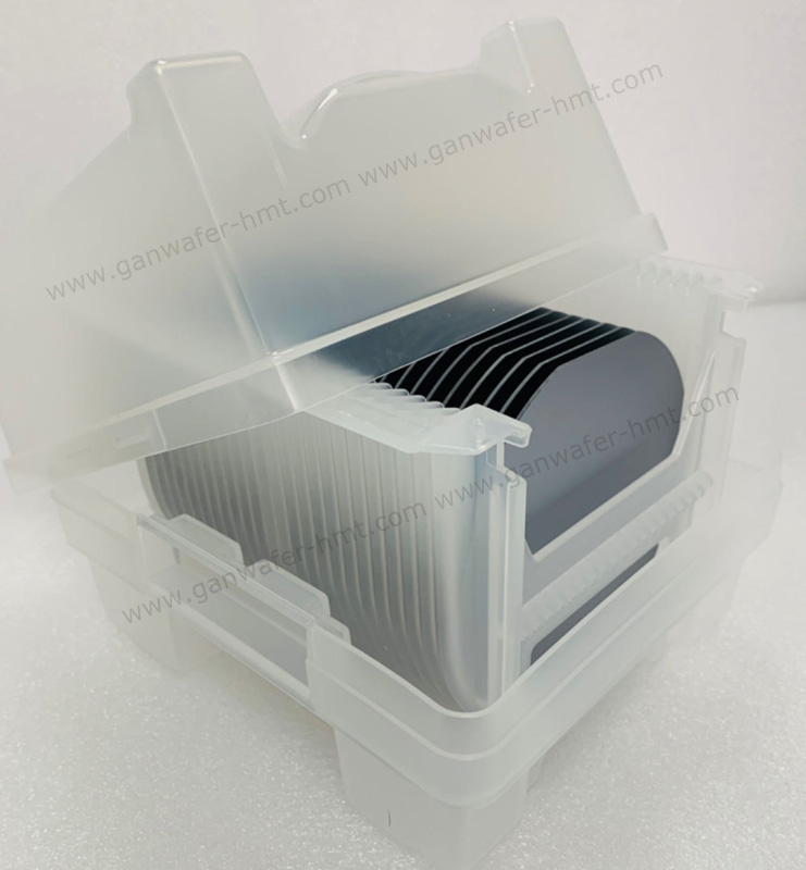
pGaN On Si Epi Wafer
GaN/AlGaN/p-GaN E-mode
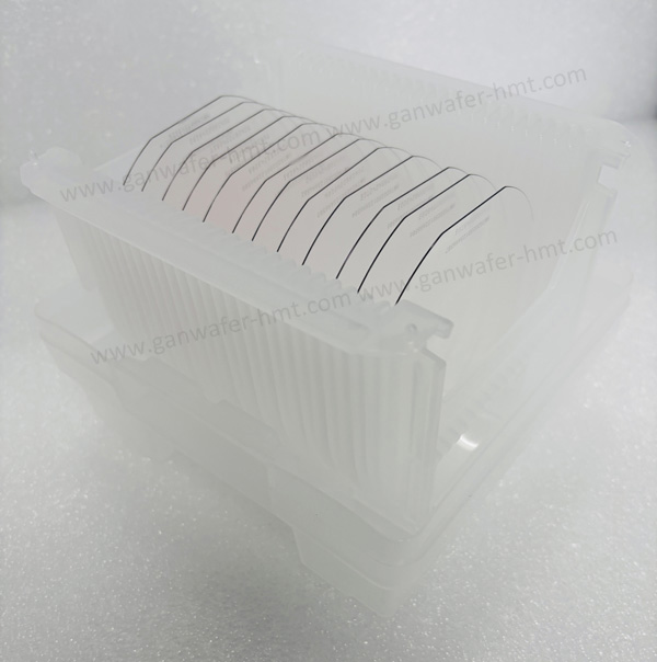
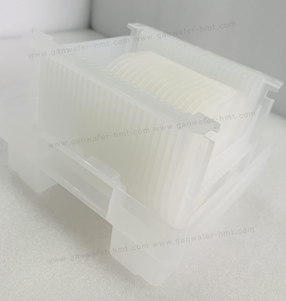
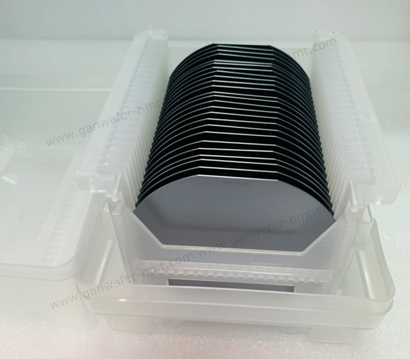
Dimension: 4 inch 6 inch 8 inch
Substrate Thichkness: 675um 1000um
Epi layer total thickness: 2~5.5um
Product Description
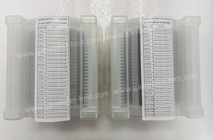
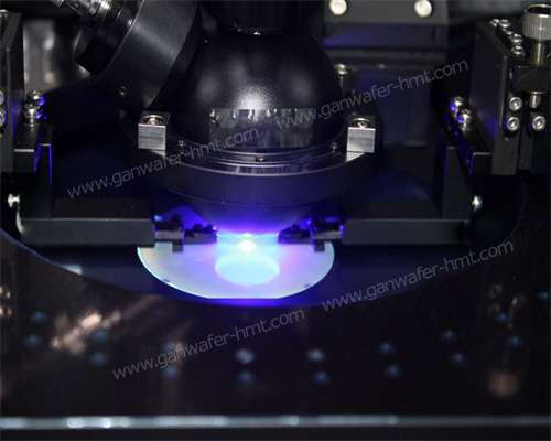
Find high quality of GaN-on-Si epi wafer manufacturer and supplier from HMT company. We supply pGaN-on-Si epi wafer with AlGaN/GaN hetero-epitaxial layer structure grown on a Silicon (111) substrate for power device application. We also supply GaN-on-SiC Epitaxy wafer for RF application.We have complete production line of 100/150/200mm GaN Epi Wafer products. We have complete and independent supporting system, including epi growth,clean,test and maintain equipments.
 Because the third generation semiconductor GaN has a wider band gap, higher breakdown electric field, higher thermal conductivity, higher electron saturation rate and better anti-irradiation ability, it is more suitable for the production of high temperature, high frequency, high power and anti-irradiation devices, and can be widely used in high pressure, high frequency, high temperature and high reliability and other fields. Including radio frequency communication, radar, satellite, power management, automotive electronics, industrial power electronics, etc.
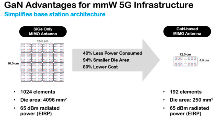
GaN Application-5G Infrastructure
GaN power amplifiers and microwave RF devices are mainly used in 5G infrastructure. GaN materials have advantages in high temperature resistance, high voltage resistance and high current resistance, and have better power efficiency, power density and broadband signal processing capabilities than traditional communication chips, which is more suitable for 5G infrastructure.
Related Products
 Homray Material Technology. All rights Reserved.
![]() E-mail:kim@homray-material.com;tina@homray-material.com
E-mail:kim@homray-material.com;tina@homray-material.com
![]() M.P: +86-15366208370 ; +86-15366203573
M.P: +86-15366208370 ; +86-15366203573