
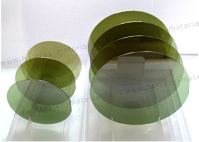
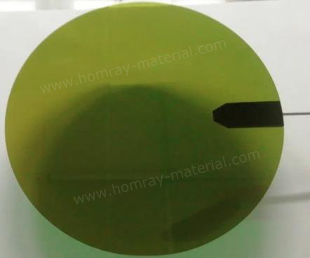
4H-SiC Wafer 4H-N/4H-SI Manufacturer
Grade: D R P
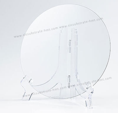
Dimension: 2 inch to 8 inch
Type: 4H-N ; 4H-SI
Thickness: 350um 500um
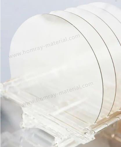
Product Description
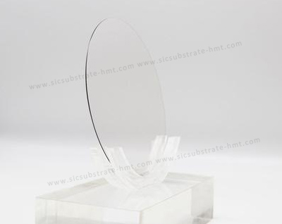
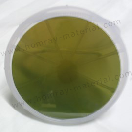
As you know, most 4H-SiC Wafer manufacturers only supply standard spec of 4H-SiC substrate, but HMT company considering the different research and application requirements of SiC wafer need different specifications, so we support customization all dimension SiC Wafers. For example, our P grade SiC Wafer normal TTV is <10um, we can customized TTV parameter upon customer requirements. Just tell your SiC wafer detailed requirements, our professional technicians will do their best to meet your requirements!
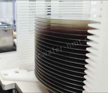
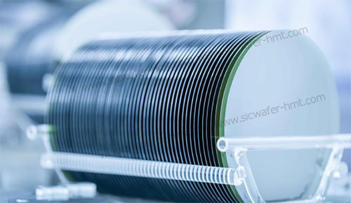
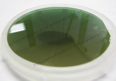
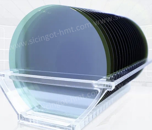
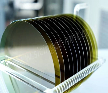
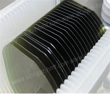
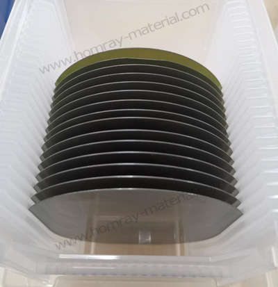
Not only SiC Substrate wafer,but also Raw Cut SiC Wafer. We can supply different thickness of As Cut SiC Wafers based on your demand. Nonstandard unpolished SiC Wafer 800um 900um or 1000um etc all OK for us.
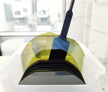
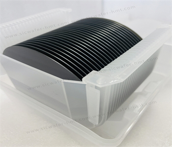
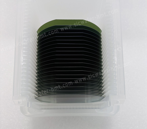
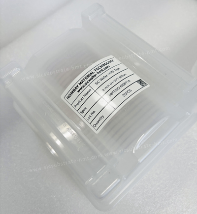
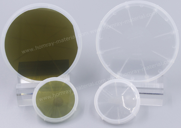
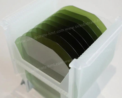
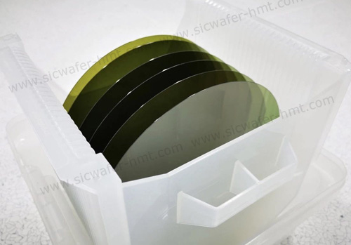
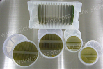
SiC Wafer In Cassette As Cut SiC Wafer In Cassette

In the field of new energy vehicles: mainly used in PCU (power control unit) and OBC (charging unit), compared with silicon devices, silicon carbide devices can reduce the weight and volume of PCU devices, reduce switching losses, and improve the operating temperature and system efficiency of the devices; Improve the power level of OBC unit, simplify the circuit structure, improve the power density, and improve the charging speed.
Photovoltaic power generation field: silicon carbide material has lower on-resistance, gate charge and reverse recovery charge characteristics, the use of silicon carbide device photovoltaic inverter, the conversion efficiency can be increased from 96% to 99%+, energy loss reduced by 50%+, equipment cycle life increased by 50 times.
Related Products

 Homray Material Technology. All rights Reserved.
![]() E-mail:kim@homray-material.com;tina@homray-material.com
E-mail:kim@homray-material.com;tina@homray-material.com