
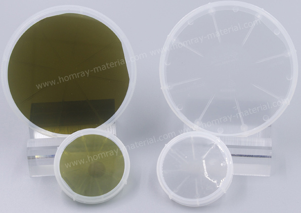
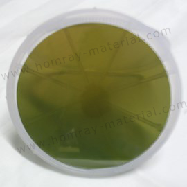
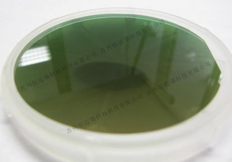
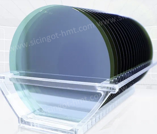
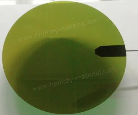
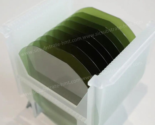
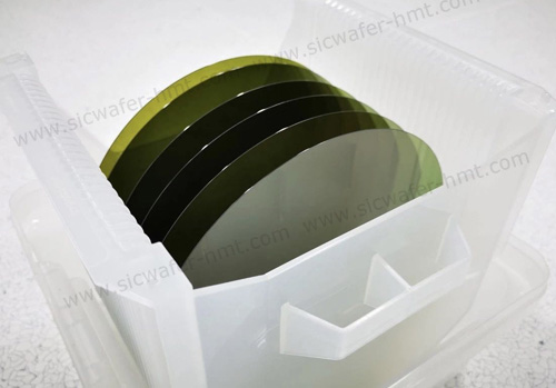
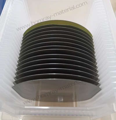
Optics SiC Wafer Manufacturer
Type: Optics SiC
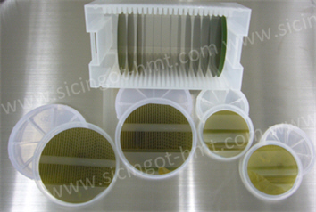
Diameter:150mm/200mm
Grade: Production
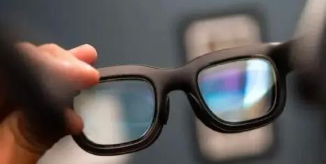
Application: AR AI
Product Description
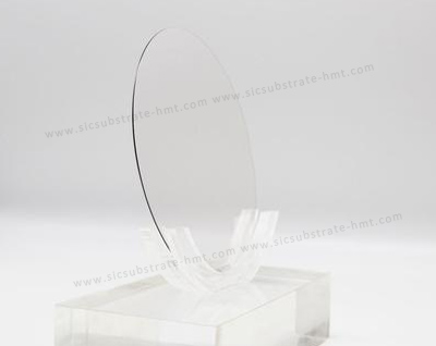
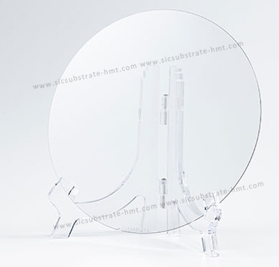
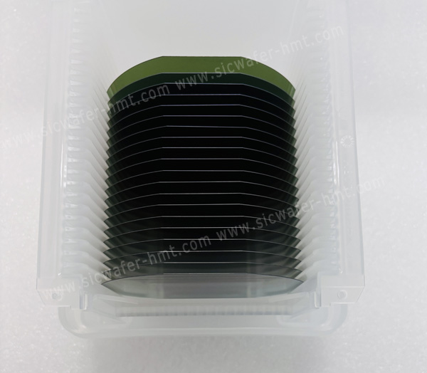
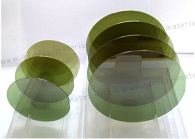
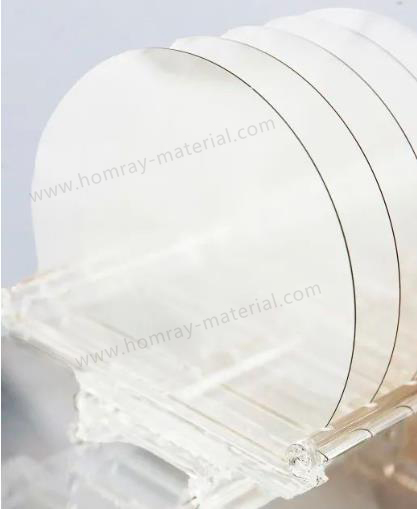
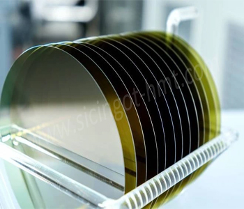
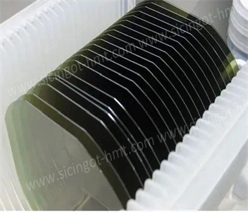
HMT proudly manufactures high-precision Silicon Carbide (SiC) wafers, As dedicated Optics SiC Wafer Manufacturers, we deliver 6inch and 8 inch SiC substrates with outstanding surface quality, minimal defects, and customizable specifications to form the reliable foundation for your next-generation AR AI Glasses.
Leveraging SiC's exceptional material properties—including superior thermal conductivity, extreme hardness, and excellent thermal stability—our wafers provide the perfect substrate for high-performance optics and robust semiconductor devices.
Optcis SiC Wafer Material Features:
1. Extremely High Refractive Index (n ≈ 2.65)
Glass: n ~ 1.5
SiC: n ~ 2.65
What does this mean?
A single-layer SiC waveguide can achieve a field of view (FOV) exceeding 80°
(Glass typically requires three layers to achieve only about 40° FOV).
2. Exceptional Thermal Conductivity (490 W/m·K)
Glass: ~1 W/m·K
SiC: 490 W/m·K
What does this mean?
High-brightness MicroLED combined with SiC waveguides ensures no overheating or discomfort on the face, significantly improving battery life and display clarity.
3. Capable of Grating Etching to Eliminate Rainbow Effects
SiC’s hardness and stability enable sub-micron grating etching, reducing the "rainbow effect"—a major weakness of Surface Relief Gratings (SRG)—by 40–60%.
The future of AR is the future of SiC.SiC + SRG + etching technology = the most advanced AR optical foundation for the next 5 years.And semi-insulating SiC substrates will lead this breakthrough! Contact us immediately and disscuss your AR AI projects.
Related Products


 Homray Material Technology. All rights Reserved.
![]() E-mail:kim@homray-material.com;tina@homray-material.com
E-mail:kim@homray-material.com;tina@homray-material.com