
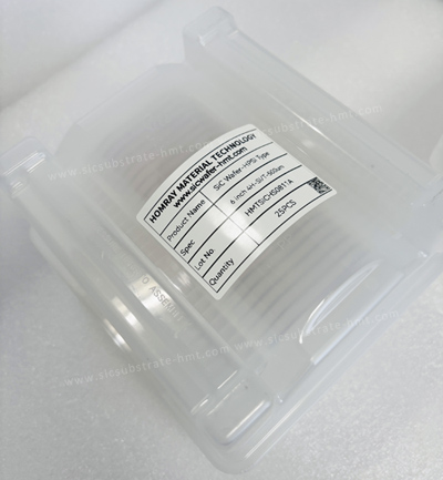
Customized SiC Wafer Manufacturer
Grade: Customization
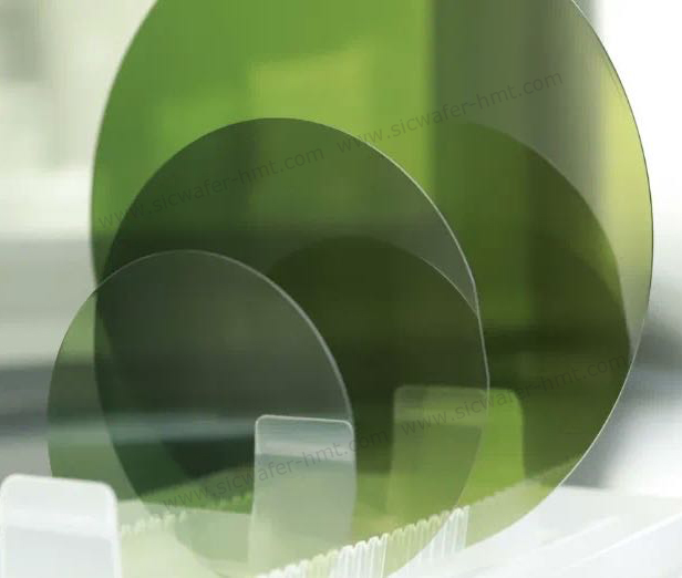
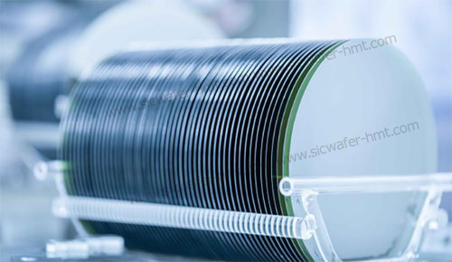
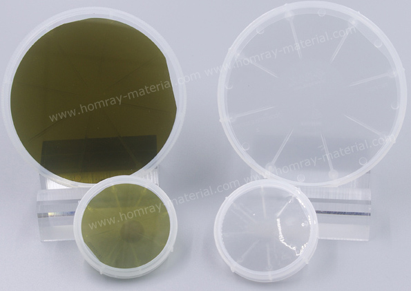
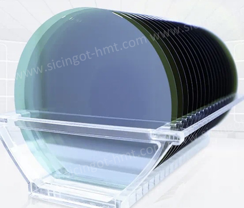
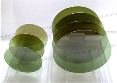
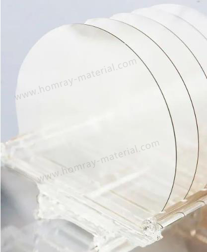
2inch 4inch 6 inch 8 inch
Thickness: Customized
Surface: Customized
Product Description
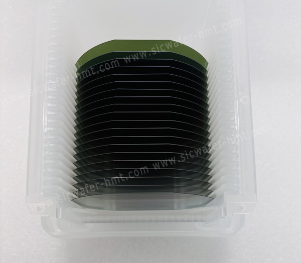
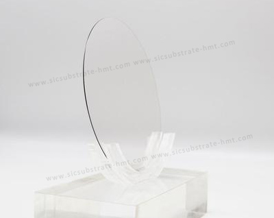
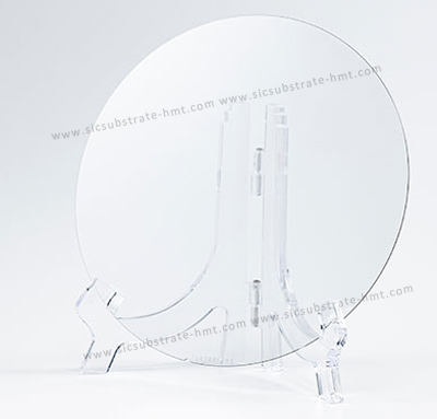
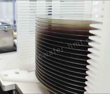
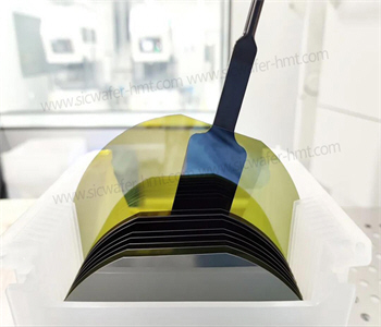
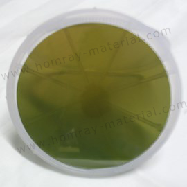
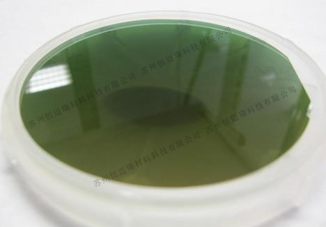
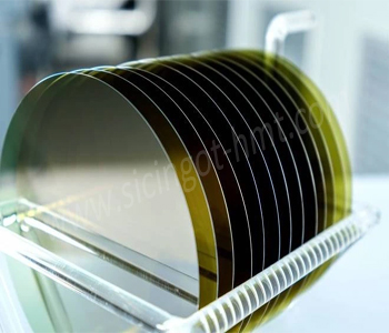
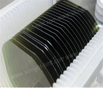
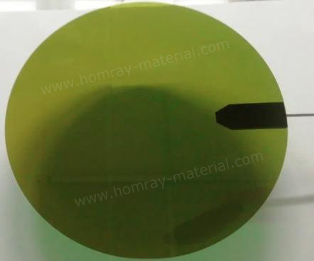
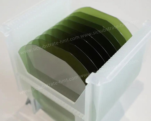
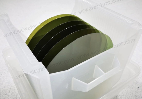
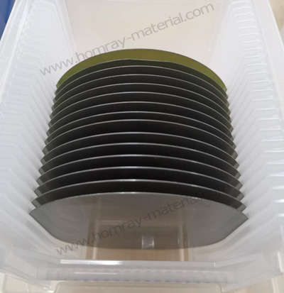
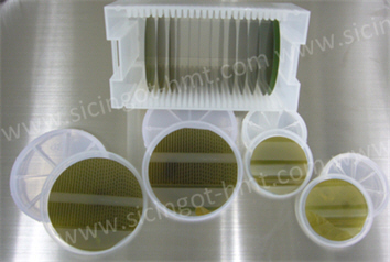
As a professional Customized SiC Wafer Manufacturers, we provide high-quality 4H-Silicon Carbide (SiC) wafers for specific R&D and mass production requirements. Our wafers are available in 2 inch, 4 inch, and 6 inch 8 inch diameters, offering both semi-insulating and N-type conductive grades. With precise control over crystal orientation, micropipe density (MPD), surface roughness, and thickness, we enable next-generation power devices, RF components, and micro-LED applications.
Key Customization SiC Wafer Parameters:
1. Wafer Size & Thickness
-
2 inch (50.8 mm): Thickness 350 µm ± 25 µm/ As-cut SiC Wafer thickness 900~1500um
-
4 inch (100 mm): Thickness 350 µm ± 25 µm/ 500±25um
- 6 inch (150 mm): Thickness 350 µm ± 25 µm/ 800±25um
2. Other customized parameters
-
TTV, BOW, Warp
- Primary flat lenght
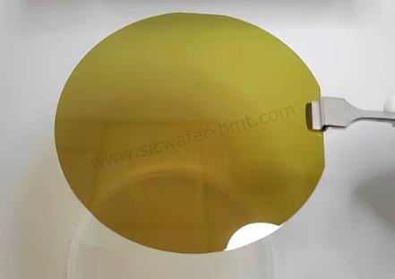
3. Surface Finish
-
Single-side polished (SSP) or Double-side polished (DSP)
-
Surface finish: Rms < 0.2 nm, 0.5nm or <1 nm
- Backside finish: As-cut, lapped, or CMP polished available
4. Defect Control (Zero Defect Option)
- Micropipe Density (MPD): < 0.5 /cm²
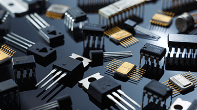

Target Applications:
-
SiC & GaN Power Devices (SBDs, MOSFETs)
-
5G RF Filters & HEMTs
-
Micro-LED Mass Transfer Substrates
-
Quantum Computing Research
-
Optical Components (Windows, Mirrors)
Why Choose Us?
With expertise in customized SiC Wafer manufacturing, we eliminate the “one-size-fits-all” constraint. Whether you require non-standard thickness, extreme flatness, or specific resistivity windows, our engineering team collaborates with you to deliver wafers that fit your process—not the other way around.
Related Products

 Homray Material Technology. All rights Reserved.
![]() E-mail:kim@homray-material.com;tina@homray-material.com
E-mail:kim@homray-material.com;tina@homray-material.com